44
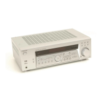
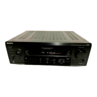
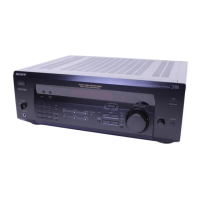
STR-DE598/DE698/DV10
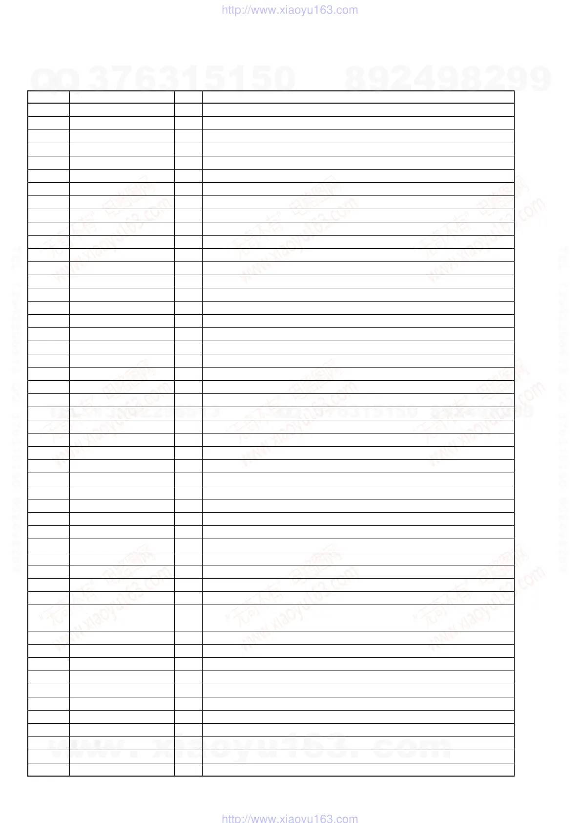
IC1101 MB90488BPF-G-137E1 (SYSTEM CONTROL) (DIGITAL Board (4/4)) (STR-DE598)
IC1101 MB90488BPF-G-110E1 (SYSTEM CONTROL) (DIGITAL Board (4/4)) (STR-DE698/DV10)
Pin No. Pin Name I/O Pin Description
1DATAO I Serial data line signal input from DIR IC
2GP9 I GP9 signal input from DSP IC
3 BST O Boot stop control signal output for DSP IC
4 HCS O Chip select signal output for DSP IC
5HACNIAcknowledge signal input from DSP IC
6 XRST O Reset signal output for DSP IC
7PMOPLL control signal output for DSP IC
8 GP12 O GP12 signal output for DSP IC
9 PCM1800_RST O Reset signal output for ADC IC
10 PCM1608_RST O Reset signal output for 8CH DAC IC
11 VSS — Ground
12 PCM1608_ML O Serial latch signal output for 8CH DAC IC
13 PCM1608_MC O Serial clock signal output for 8CH DAC IC
14 PCM1608_MDI O Serial data output for 8CH DAC IC
15 PCM1608_MDO I Serial data input from 8CH DAC IC
16 T.SERIAL_CLK O Serial clock signal output for tuner pack
17 TUNER_DATA O Serial data output for tuner pack
18 HDOUT I Serial data input from DSP IC
19 HDIN O Serial data output for DSP IC
20 HCLK O Serial data clock signal output for DSP IC
21 DLY_BYPASS O Bypass signal output for DAC IC (STR-DE698/DV10 only)
22 DIR/AD O A/D port signal output for DIR IC (STR-DE698/DV10 only)
23 VCC5 — Power supply pin (+3.4 V)
24 SYS_MUTE O System mute control signal output
25 ANA/DIG O Analog/Digital port signal output
26 UPCON_RST O Not used (Open)
27 FLASH2_VOL/VOL_CLK O Flash programming signal output 2/Volume clock signal output
28 FLASH1/VOL_DATA_LATCH O Flash programming signal output 1/Volume data latch signal output
29 SDA I/O Serial data input/output for EEPROM IC
30 SCL O Clock signal output for EEPROM IC
31 ENC_A O Menu encoder (A) signal output (STR-DE698/DV10 only)
32 ENC_B O Menu encoder (B) signal output (STR-DE698/DV10 only)
33 UPCON O Serial data output for Y/C separation IC (STR-DE698 only)
34 UPCON_CLK O Clock signal output for Y/C separation IC (STR-DE698 only)
35 AVCC — Power supply pin (+3.4 V)
36 AVRH — Power supply pin (+3.4 V)
37 AVSS — Ground
38 to 40 A/D0 to A/D2 I Key signal input (A/D port)
41 VERSION I
Destination detection signal input (Fixed at L: US, Canadian model, H: Except US,
Canadian model)
42 VSS — Ground
43 RDS_SIG I RDS signal level input (AEP, UK model only)
44 MODEL I Model detection signal input (Fixed at L: STR-DE698, H: STR-DE598/DV10)
45 VOL_ENC (A) I Volume encoder (A) signal input
46 VOL_ENC (B) I Volume encoder (B) signal input
47 BLUE_LED O LED (MULTI CHANNEL DECODING) driver signal output
48 STOP I AC off detection signal input
49 MOD0 — Selection of micon operation mode
50 MOD1 — Not used (Connect to AVCC)
51 MOD2 — Selection of micon operation mode
52 RDS_CLK I RDS data clock signal input (AEP, UK model only)
Ver. 1.1
w
w
w
.
x
i
a
o
y
u
1
6
3
.
c
o
m
Q
Q
3
7
6
3
1
5
1
5
0
9
9
2
8
9
4
2
9
8
T
E
L
1
3
9
4
2
2
9
6
5
1
3
9
9
2
8
9
4
2
9
8
0
5
1
5
1
3
6
7
3
Q
Q
TEL 13942296513 QQ 376315150 892498299
TEL 13942296513 QQ 376315150 892498299
http://www.xiaoyu163.com
http://www.xiaoyu163.com