10
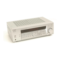
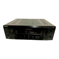
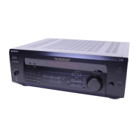
STR-DE598/DE698/DV10
• IC Pin Description
IC1101 TMP92CY23FG-6F96(JZ (SYSTEM CONTROL) (DIGITAL Board (4/4)) (STR-DE698: US model)
Pin No. Pin Name I/O Pin Description
1AVSS — Ground
2AVCC — Power supply pin (+3.4 V)
3 RDS_DATA I RDS data input (Fixed at L)
4POWER_KEY I Power key detection signal input
5STOPIAC off detection signal input
6 SIRCS I SIRCS signal input
7 HDIN O Serial data output for DSP IC
8 HDOUT I Serial data input from DSP IC
9 HCLK O Serial data clock signal output for DSP IC
10 FLASH1/UPCON_RST O Flash programming signal output 1
11 FLASH2/ANA/DIG O Flash programming signal output 2/Analog/Digital port signal output
12 SW1 O Video select signal output 1
13 NTSC_PAL_SW O NTSC/PAL switch signal output
14 SDA I/O Serial data input/output for EEPROM IC
15 SCL O Clock signal output for EEPROM IC
16 UPCON I/O Serial data input/output for Y/C separation IC
17 UPCON_CLK O Clock signal output for Y/C separation IC
18 SW2 O Video select signal output 2
19 COMPO_SW2/A1_IN O COMPONENT VIDEO switch 2 signal output
20 DVSS — Ground
21 RDS_CLK I RDS data clock signal input (Fixed at L)
22 DVCC — Power supply pin (+3.4 V)
23 FRONT_RY O Front speaker A relay driver control signal output
24 SP_B_RY O Front speaker B relay driver control signal output
25 C/SB_RY O Center speaker relay driver control signal output
26 REAR_RY O Surround speaker relay driver control signal output
27 COMPO_SW1/A1_OUT O COMPONENT VIDEO switch 1 signal output
28 SW_RY O Sub woofer relay driver control signal output
29 BRIDGEABLE_RY O Bridgeable relay driver control signal output
30 TUNER_DATA O Serial data output for tuner pack
31 T.SERIAL_CLK O Serial clock signal output for tuner pack
32 DO I Tuner serial data input
33 SLATCH O Tuner latch signal output
34 TUNED I Tuned signal detection input
35 STEREO I Stereo signal detection input
36 MUTE O Tuner mute signal output
37, 38 SW3, SW4 O Video select signal output 3, 4
39 DVSS — Ground
40 NMI — Not used (Fixed at L)
41 DVCC — Power supply pin (+3.4 V)
42 SELECT2 O Digital input select 2 signal output
43 SELECT1 O Digital input select 1 signal output
44 BST_SEL O 96/24 signal output for DSP IC
45 XMODE O Xmode signal output for DIR IC
46 CKSEL1 O Clock select signal output for DIR IC
47 CLK O Data clock signal output for DIR IC
48 CE O Latch signal output for DIR IC
49 DI O Data output for DIR IC
50 DO I Data input from DIR IC
51 ERROR I Error detection signal input from DIR IC
52 XSTATE I Xstate signal input from DIR IC
w
w
w
.
x
i
a
o
y
u
1
6
3
.
c
o
m
Q
Q
3
7
6
3
1
5
1
5
0
9
9
2
8
9
4
2
9
8
T
E
L
1
3
9
4
2
2
9
6
5
1
3
9
9
2
8
9
4
2
9
8
0
5
1
5
1
3
6
7
3
Q
Q
TEL 13942296513 QQ 376315150 892498299
TEL 13942296513 QQ 376315150 892498299
http://www.xiaoyu163.com
http://www.xiaoyu163.com