– 4 –
SECTION 1
SERVICING NOTE
MEASURING VOLTAGE AND WAVEFORM
Measure the voltage and waveform of this unit at the following conditions.
Connection Diagram:
Procedure:
1. Perform initialization. (Refer to the following.)
2. Rotate the INPUT SELECTOR knob and select CD.
3. Set the MASTER VOLUME to -20 dB.
4. Using a YEDS-18 disc (3-702-101-01), etc., input the reference signal 1 KHz 0 dB (Lch + Rch) into “CD DIGITAL Input”.
(It is recommended that the CD player be set to the 1-track repeat mode during playback.)
Initialization
Mode for initializing the state for setting the unit .
1. Press the MAIN MENU button to display “<<<CUSTOMIZE>>>”.
2. Rotate the MENU knob to display “MEMORY CLEAR[NO]”.
3. Rotate the +/– knob to display “MEMORY CLEAR[YES]”.
4. After about 1 second, “Are you sure [NO]” will be displayed. Rotate the +/– knob to display “Are you sure [YES]”.
5. After about 1 second, the power goes off automatically and initialization is executed. After this, the power turns on again.
1. SERVICING NOTE .......................................................... 4
2. GENERAL .......................................................................... 5
3. ELECTRICAL ADJUSTMENT ................................. 11
4. DIAGRAMS
4-1. Circuit Boards Location ...................................................... 12
4-2. Block Diagrams
• Video Section ................................................................... 13
• S-Video Section ............................................................... 15
• Analog (1/3) Section ........................................................ 17
• Analog (2/3) Section ........................................................ 19
• Analog (3/3) Section ........................................................ 21
• Digital (DIR/ADC) Section ............................................. 23
• Digital (DSP) Section ...................................................... 25
• Digital (CPU (1/2)) Section ............................................. 27
• Digital (CPU (2/2)) Section ............................................. 29
• Digital (SRC/DAC) Section ............................................. 31
• Digital (IDAC/OUT) Section........................................... 33
• Display Section ................................................................ 35
• AC-3RF Section............................................................... 37
• Power Section .................................................................. 39
4-3. Schematic Diagram – Video Section –................................ 43
4-4. Printed Wiring Board – Video Section – ............................. 45
4-5. Schematic Diagram – (S) Video Section –.......................... 47
4-6. Printed Wiring Board – (S) Video Section – ....................... 49
4-7. Schematic Diagram – Analog (1/3) Section –..................... 51
4-8. Schematic Diagram – Analog (2/3) Section –..................... 53
4-9. Schematic Diagram – Analog (3/3) Switch Section – ........ 55
4-10. Printed Wiring Board – Analog Section – ........................ 57
4-11. Printed Wiring Board – Digital Section – ........................ 59
4-12. Schematic Diagram – Digital (1/8) Section – .................. 63
4-13. Schematic Diagram – Digital (2/8) Section – .................. 65
4-14. Schematic Diagram – Digital (3/8) Section – .................. 67
4-15. Schematic Diagram – Digital (4/8) Section – .................. 69
4-16. Schematic Diagram – Digital (5/8) Section – .................. 71
4-17. Schematic Diagram – Digital (6/8) Section – .................. 73
4-18. Schematic Diagram – Digital (7/8) Section – .................. 75
4-19. Schematic Diagram – Digital (8/8) Section – .................. 77
4-20. Schematic Diagram – Display (1/2) Section – ................. 79
4-21. Schematic Diagram – Display (2/2) Section – ................. 81
4-22. Printed Wiring Board – Display Section – ....................... 83
4-23. Schematic Diagram – AC 3RF Section – ......................... 85
4-24. Printed Wiring Board – AC 3RF Section –....................... 87
4-25. Schematic Diagram – Power Section – ............................ 89
4-26. Printed Wiring Board – Power Section – ......................... 91
4-27. Schematic Diagram – AC Input Section – ........................ 93
4-28. Printed Wiring Board – AC Input Section – ..................... 95
4-29. Schematic Diagram – Clock Section – ............................. 97
4-30. Printed Wiring Board – Clock Section – .......................... 97
4-31. IC Block Diagrams ........................................................... 98
4-32. IC Pin Functions ............................................................. 102
5. EXPLODED VIEWS
5-1. Back Panel Section ........................................................... 117
5-2. Front Panel Section ........................................................... 118
5-3. Chassis Section ................................................................. 119
6. ELECTRICAL PARTS LIST ...................................... 120
TABLE OF CONTENTS
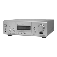
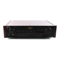
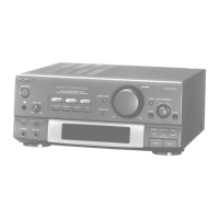
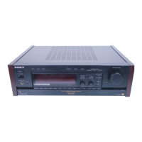
TA-E9000ES
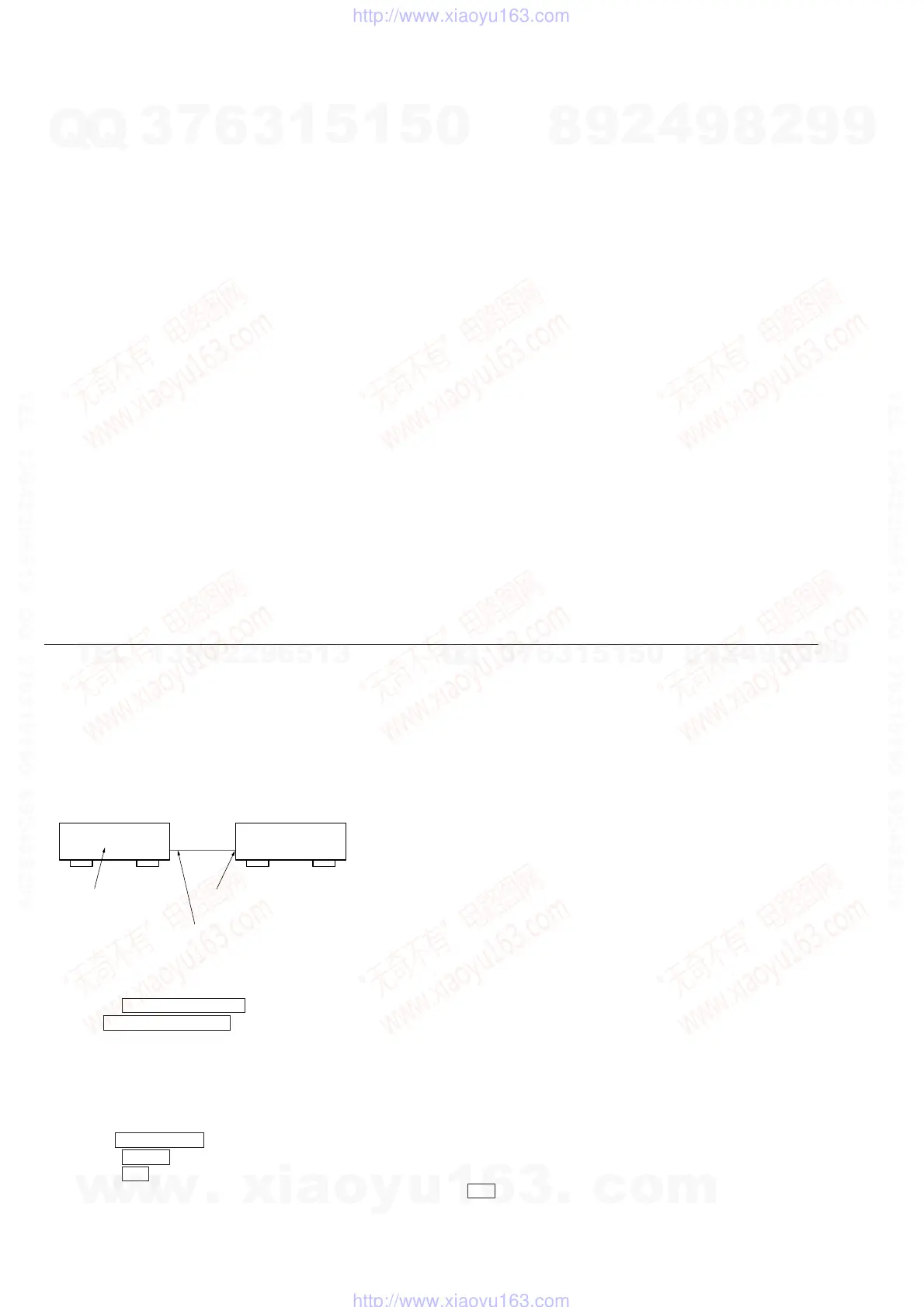
CD player with
optical digital output
Optical digital cable
(Optional accessory)
CD DIGITAL input
w
w
w
.
x
i
a
o
y
u
1
6
3
.
c
o
m
Q
Q
3
7
6
3
1
5
1
5
0
9
9
2
8
9
4
2
9
8
T
E
L
1
3
9
4
2
2
9
6
5
1
3
9
9
2
8
9
4
2
9
8
0
5
1
5
1
3
6
7
3
Q
Q
TEL 13942296513 QQ 376315150 892498299
TEL 13942296513 QQ 376315150 892498299
http://www.xiaoyu163.com
http://www.xiaoyu163.com