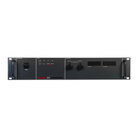
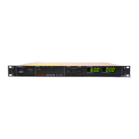
SORENSEN DCS SERIES MANUAL THEORY OF OPERATION
3-5
Models DCS 150-7, DCS 300-3.5 and DCS 600-1.7
On DCS 150-7 and DCS 300-3.5, diodes CR301-CR304 form the rectifier bridge with resistors R301-R304 and
capacitors C301-C304 providing snubbing for the diodes. Resistor R305 and capacitor C305 form the snubber on
the secondary of transformer T1. Capacitor C306 provides bypassing on the output of the bridge.
On DCS 600-1.7, diodes CR300-CR307 form the rectifier bridge with resistors R302-R305 and capacitors
C1,2,4-13 providing snubbing for the diodes. Resistor R300 and R301 and capacitor C303 form the snubber on the
secondary of transformer T1. Capacitor C300 provides bypassing on the output of the bridge.
Voltage Control Circuit
The output voltage is monitored by the voltage control op amp U5 at pin 3 via the positive sense line (pin 13 of
connector J3 on 8V to 80V models) and the resistor divider formed by R21, R22, R53, R85 and R147. This
feedback voltage is compared with a 0-5V reference voltage gated from the front panel voltage control to pin 2 of
U5 by U7-2 to provide an error signal for the PWM. If the output voltage tries to rise above the selected level the
voltage at pin 3 rises and the output of U5 becomes more positive. This increase is applied to the inverting input of
the PWM error amplifier through diode CR18 and resistor R69 causing the amplifier output to decrease. This
reduces the PWM output drive waveform pulse width, lowering the output voltage and regulating the output at the
desired level. Similarly, if the output voltage tries to fall below the selected level the voltage at pin 3 decreases, U5
output decreases, the output from the PWM error amplifier increases and the drive waveform pulse width increases
which raises the output voltage to the desired level. During voltage mode operation the output of the current
control circuit at U4-1 pin 1 remains low. Resistor R70 and capacitor C54 provide compensation for the op amp
and diode CR21A limits saturation. Capacitor C20, resistor R54 and CMOS gate U7-3 provide a soft start for the
power supply during initial startup and recovery from shut down conditions by delaying the voltage rise at pin 2 of
U5. Resistor R21 supplies the front panel voltmeter with a voltage proportional to the output voltage through pin 6
of the J1 connector while a buffered 0-5V signal (uncalibrated) for remote monitoring of the output voltage is
provided at pin 19 of connector J3. Potentiometer R53 is used to adjust the full scale output of the power supply
and potentiometer R52 is used to adjust the offset on op amp U5.
Current Control Circuit
The output current is monitored by current shunt resistor R91 which develops a voltage across it proportional to the
output current. This voltage is amplified and conditioned by the differential op amp U15 and associated
components to provide a control ground referenced 0-2V signal at pin 3 of the current control op amp U4-1. This
signal is compared to a reference signal gated from the front panel current control to pin 2 of U4-1 by U7-1. As
the output current increases the voltage at pin 3 rises until it reaches the reference level set at pin 2 at which time
the output of U4-1 goes high and the unit switches from voltage mode to current mode operation. The output
current is maintained at the desired level by providing negative feedback to the PWM error amplifier as described
in the voltage control circuit description above. Resistor R27 and capacitor C27 provide compensation for U4-1.
Op amp U4-2 and related components scale the current feedback signal to provide a calibrated 0-5V output at pin 7
of connector J3 for external monitoring of the output current. The shunt voltage is also fed to the front panel
ammeter via pins 8 and 9 of connector J1.
Operating Mode Indicator Circuit
Op amp U8-2 takes advantage of the fact that diode CR18 is forward biased during voltage mode and reverse
biased during current mode to provide a mode indication signal at pin 7. This output is used to drive the back to
back mode LEDs on the front panel through pin 1 of connector J1. In voltage mode U8-2 pin 7 is high and the
green voltage mode led is illuminated. In current mode pin 7 is low and the red current mode led is illuminated.
www.valuetronics.com