DocID026304 Rev 3 17/44
AN4488 Power supplies
43
The following conditions must be respected:
• V
DD
should always be higher than V
CAP
to avoid current injection between power
domains.
• If the time for V
CAP
to reach V12 minimum value is smaller than the time for V
DD
to
reach 1.7 V, then PA0 should be kept low to cover both conditions: until V
CAP
reaches
V12 minimum value and until V
DD
reaches 1.7 V.
• Otherwise, if the time for V
CAP
to reach V12 minimum value is smaller than the time for
V
DD
to reach 1.7 V, then PA0 could be asserted low externally.
• If V
CAP
goes below V12 minimum value and V
DD
is higher than 1.7 V, then PA0 must
be asserted low externally.
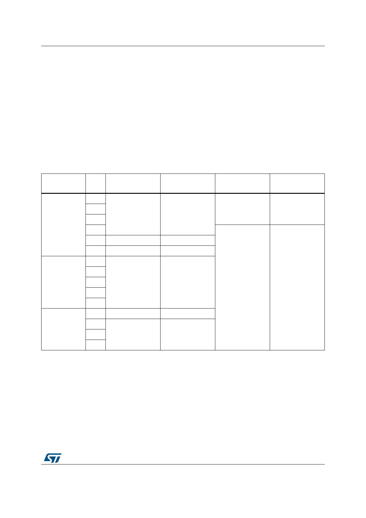
2.3.7 Regulator ON/OFF and internal reset ON/OFF availability
Table 3. Regulator ON/OFF and internal power supply supervisor availability
Package pins Regulator ON Regulator OFF
Power supply
supervisor ON
Power supply
supervisor OFF
Packages with
pins on 4 edges
48
Yes
(1)
No
Yes
(2)
No64
100
144
Yes
PDR_ON set to V
DD
Yes
PDR_ON external
control
(3)
176 Yes
(4)
Yes
(5)
208 Yes
(1)
No
BGA Packages
100
Yes
(4)
Yes
(5)
144
169
176
216
Chip Scale
Packages
49 Yes
(1)
No
81
Yes
(4)
Yes
(5)
90
143
1. BYPASS_REG internally connected to V
SS
2. PDR_ON internally connected to V
DD
3. PDR_ON can be permanently set to VSS for STM32F411xx and STM32F446xx devices. For other devices, see Chapter
2.3.4
4. BYPASS_REG set to V
SS
5. BYPASS_REG set to V
DD

 Loading...


