Package AN4488
20/44 DocID026304 Rev 3
3.2 Pinout Compatibility
Table 6 allows to select the right package depending on required signals. Note the two
different pinouts for 64 and 100 pins which require specific connection in case board
compatibility is required. See Table 10 and 11.
Note that Chip Scale Package of different products even with same pinout might have
different package dimensions which might be taken into account for PCB clearance. See
Table 5.
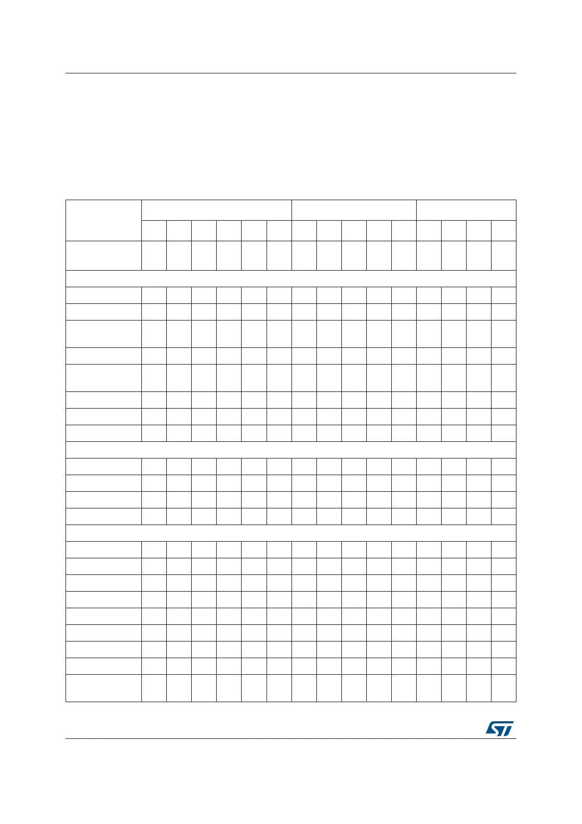
Table 6. Pinout summary
Pin Name
xQFP/xQFN xBGA xCSP
48 64 100 144 176 208 100 144 169 176 216 49 81 90 143
Number of IOs 36
51
(1)
50
(2)
82
(1)
81
(2)
114 140 168 81 114 130 140 168 36 63 72 114
Specific IOs availability
PA0-WKUP XXXXXXXXXXXXXXX
PB2-BOOT1 XXXXXXXXXXXXXXX
PC13-
ANTI_TAMP
XXXXXXXXXXXXXXX
PC14-OSC32_INXXXXXXXXXXXXXXX
PC15-
OSC32_OUT
XXXXXXXXXXXXXXX
PH0 - OSC_INXXXXXXXXXXXXXXX
PH1 - OSC_OUTXXXXXXXXXXXXXXX
PI8- ANTI TAMP2 ----XX---XX----
System related pins
BOOT0 XXXXXXXXXXXXXXX
NRST XXXXXXXXXXXXXXX
BYPASS_REG - - - - X XXXXX XXX
PDR_ON - - - XXXXXXXXXXXX
Supplies pins
VBAT XXXXXXXXXXXX - XX
VDDA - - XXXXXXXXX - - - X
VREF+ - - XXXXXXXXX - - - X
VDDA/VREF+XX---------XXX
VSSA - - - - - - XXXXX - - - -
VREF- - - - - - - XXXXX - - - -
VSSA/VREF-XXXXXX-----XXXX
VDDUSB33 - - - X
(3)
---X----X--
number of VDD
(4)
346
12
(1)
11
(5)
1517 4 12141418 3 5 5 13

 Loading...


