DocID026304 Rev 3 9/44
AN4488 Power supplies
43
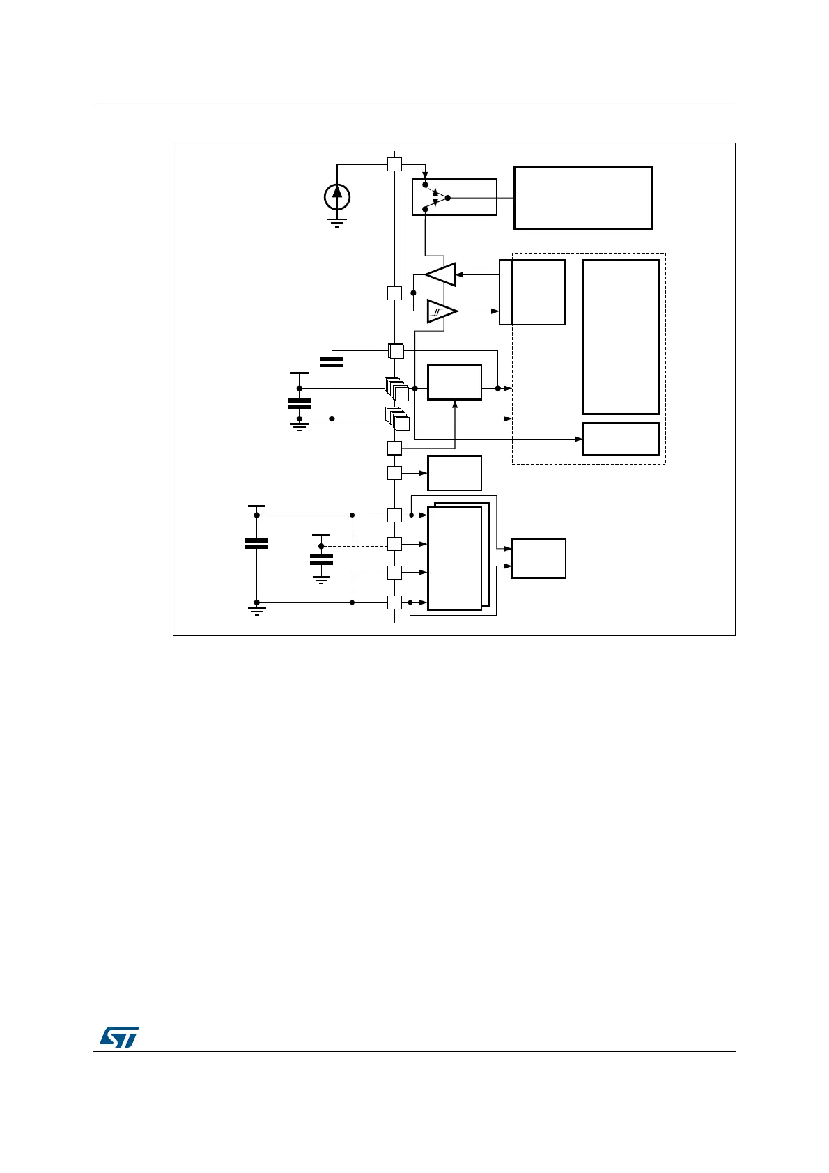
Figure 1. Power supply scheme
1. Optional. If a separate, external reference voltage is connected on V
REF+
, the two capacitors (100 nF and
1 µF) must be connected.
2. V
CAP2
is not available on all packages. In that case, a single 4.7 µF (ESR < 1Ω) is connected to V
CAP1
3. V
REF+
is either connected to V
REF+
or to V
DDA
(depending on package).
4. V
REF-
is either connected to V
REF-
or to V
SSA
(depending on package).
5. N is the number of V
DD
and V
SS
inputs.
6. Refer to section “Voltage regulator” in datasheet (Table 1) to connect BYPASS_REG and PDR_ON pins.
3RZHUVZLWFK
%DFNXSFLUFXLWU\
26&.57&
:DNHXSORJLF
%DFNXSUHJLVWHUV
%DFNXS5$0
.HUQHOORJLF
&38
GLJLWDO
5$0
/HYHOVKLIWHU
$QDORJ
5&V3//
069
9
''
1
9
%$7
287
,1
1îQ)
î)
9%$7
WR9
9ROWDJH
UHJXODWRU
9
66
1
9
''$
9
5()
9
5()
9
66$
$'&
9
''
)
9
5()
Q)
)
9
''
)ODVKPHPRU\
9
&$3
9
&$3
î)
%<3$66B5(*
3'5B21
5HVHW
FRQWUROOHU
Q)
î)
QRWH
QRWH
QRWH
QRWH
*3,2V
,2
/RJLF

 Loading...


