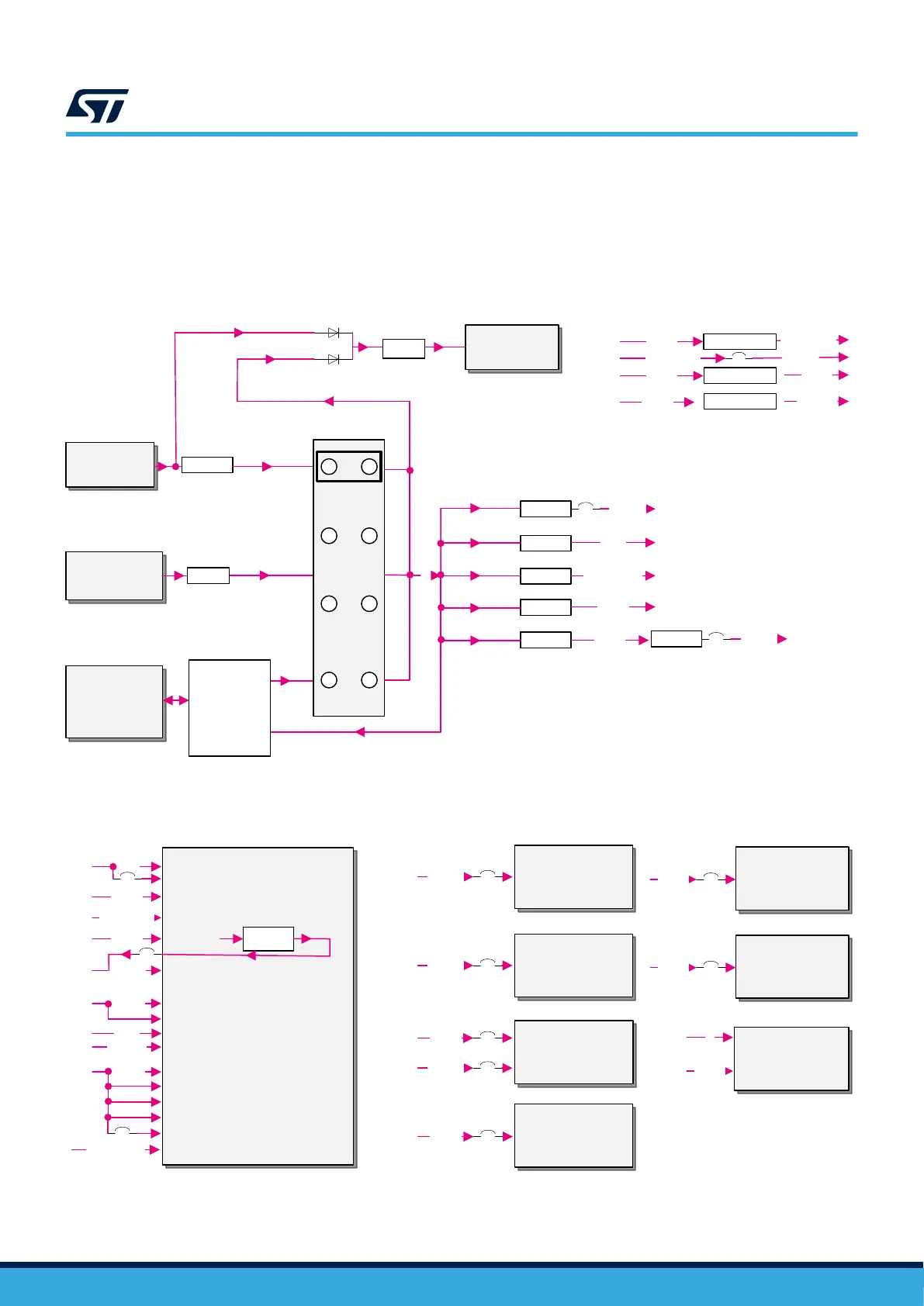
7.4 Power supply
Figure 7 describes the power architecture and the maximum voltage and current limits, under which functions can
be safely used on the STM32N6570-DK product. In any case, ensure the total power budget of the application
always conforms to the selected 5 V power source mode, if not malfunction can occur. For detailed configuration,
refer to the relevant function description and technical application notes.
Figure 7. Power diagram
DT59552V1
USB1
Type-C
®
ARDUINO
®
USB-C
protection
for DRP
5 V/up to 0.8 A
USB
ST-LINK
eFuse
5 V/up to 3 A
5V SEL
5 V/up to 1.5 A
ST-LINK
MCU
3.3 V/up to 300 mA
STM32N657X0H3Q
Hexadeca-SPI
PSRAM
Octo-SPI
flash
Audio
Others
5V
DCDC
0.8 V
LDO
3.3 V
LDO
1.8 V
DCDC
1.8 V
DCDC
3.3 V
LDO
1.8 V
5V
VDDCORE
VDDIO
VDDA1V8_AON
VDD1V8
VDDA1V8
VDDIO
VDD
VBAT
VDD33USB
VDDSMPS
VDDA18PMU
VDDIO2
VDDA18CSI
VDD3V3
VDD1V8
VDDA1V8PMU
VDDIO3
VDDIO4
VDDIO5
VDDA1V8
VDDIO
VDDIO_SD
VDDA18USB
VDDA18ADC
VDDA18AON
VDDA18PLL
VREF+
VDDA1V8
VDDA1V8_AON
VDDCORE
VDDCORE
INTERNAL
SMPS
VDD1V8
VDDA1V8PMU
VDDA1V8PMU
VDDA1V8
VDDA1V8
VDDA1V8
VDD3V3
VDDA1V8
Ethernet
VDD3V3
SD card
VDD3V3
VDD3V3
Switch
VDD_SD
SPDT
VDD_SD
VDDIO_SD
MEMs
microphone
VDD3V3
VDD3V3
VDD3V3
5V
5V
LDO
5 V/1.5 A
LDO
Inductor
UM3300
Hardware layout and configuration
UM3300 - Rev 1
page 13/49