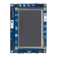
7.8 TFT color LCD 800x480 pixels
The STM32N6570-DK board includes a 5‑inch 800x480 LCD‑TFT board (MB1860), which is connected to the
RGB interface of STM32N657X0H3Q through a 50‑pin connector (CN3). The MB1860 LCD daughterboard uses a
TFT LCD with the driving system, white LED backlight, and capacitive touch panel.
The touch-panel controller interfaces with STM32N657X0H3Q via the bidirectional I2C2 bus: SCL (PD14) and
SDA (PD4). The I
2
C write‑read address is 0xBA/0xBB.
Warning: LCD_R3 (PB4) and LCD_R5 (PA15) are multiplexed with JTAG.
7.9
USB1 USB Type-C
®
(HS, DRP)
The STM32N6570-DK board supports a USB HS 2.0 interface on the USB Type-C
®
receptacle connector (CN18).
It offers compatibility with USB Type-C
®
revision 1.3, USB PD 3.0, PPS, and USB BC 1.2 on the USB Type-C
®
receptacle connector (CN18).
CN18 can be used as a DRP (dual‑role port). Its VBUS can be managed to supply other platforms as a Provider
or be supplied as a Consumer. The embedded UCPD protection manages DRP functions. It is compatible with
VBUS current up to 1.5 A and VBUS 5 V only.
By default, the embedded UCPD protection manages the dead battery (DB) feature of this USB connector. It
communicates with MCU via the bidirectional I2C2 bus: SCL (PD14) and SDA (PD4). The I
2
C write/read address
is 0x68/0x69.
The red LED (LD10) indicates the USB OCP status.
The green LED (LD9) lights up when one of the following events occurs:
• The source path is open, and STM32N6570-DK provides up to 1.5 A 5 V power to CN18.
• VBUS1 is powered by another USB host when the STM32N6570-DK board works as a Sink device.
7.10
USB2 Type-A (HS, host only)
USB2 is used as a host at high speed, and the current is limited to 0.5 A maximum. The USB2 connector (CN17)
is a USB Type-A connector.
The red LED (LD8) indicates the power fault status of USB2.
7.11
Octo‑SPI flash memory
The Octo‑SPI flash memory has the following characteristics: 1-Gbit, 1.8 V, 200 MHz, DTR, read while writing. It is
connected to the OCTOSPI interface of the STM32N657X0H3Q microcontroller on the STM32N6570-DK board.
Note: Since the NRST (system reset) is at 3.3 V level, while the reset of the flash memory is 1.8 V in this design, a
diode (D4) is used to adapt the reset signals.
7.12
Hexadeca‑SPI PSRAM
The Hexadeca‑SPI PSRAM has the following characteristics: 256 Mbits, 1.8 V, 200 MHz, DDR. It is connected to
the
Hexadeca‑SPI interface of the STM32N657X0H3Q microcontroller on the STM32N6570-DK board.
7.13
Ethernet
The STM32N6570-DK board supports 10/100/1000-Mbit Ethernet communication with a PHY and integrates an
RJ45 connector (CN16). The Ethernet PHY is connected to the STM32N657X0H3Q microcontroller via an RGMII
interface.
The 25 MHz clock of the PHY is generated from the X4 crystal.
UM3300
Hardware layout and configuration
UM3300 - Rev 1
page 17/49