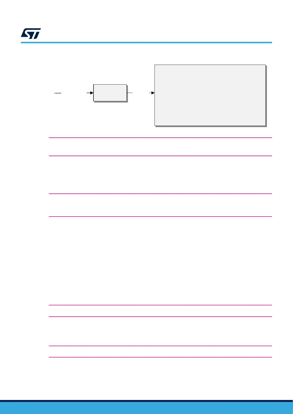
Figure 11. ADC ARDUINO
®
input voltage adaptation
DT59556V1
Amplifier
3V3 ADC from
ARDUINO
®
1V8 ADC
STM32N657X0H3Q
MCU
ADC
Warning:
USB1 ISENSE shares the same ADC with ARDUINO
®
ADC0 (A0).
STMod+ shares the same ADC (CN4 pin13) with ARDUINO
®
ADC5 (A5).
7.18 STMod+
STM32N6570-DK features STMod+.
Note:
For the ADC pin in the STMod+ connector, the same solution as for ARDUINO
®
A0 to A5 pins is adapted,
connecting two pins (one analog and one digital I/O) to the ADC pin.
Warning: STMod+ function causes the loss of an SPI on CN4 pin9 due to the lack of available SPI
resources.
STMod+ shares the same ADC (CN4 pin13) with ARDUINO
®
ADC5 (A5)
7.19
Virtual COM port
The serial interface UART1 (PE5/PE6) that supports the bootloader is directly available as a Virtual COM port of
the PC connected to the
STLINK-V3EC USB connector (CN6). The VCP configuration is the following:
• 115200 bit/s
• 8-bit data
• Even parity
• One-stop bit
• No flow control
7.20
TAG
One TAG interface footprint (CN1) is reserved on the STM32N6570-DK board, which can be used for the board
debugging and programming.
Warning: The JNRST(PB4) and MCU.JTDI(PA15) are multiplexed with LCD signals.
7.21
MIPI20
One MIPI20 connector (CN10) is on the STM32N6570-DK board, which can be used for the board debugging and
programming.
Warning: The trace signals (PB0, PB6, PB7, PE3, and PG7) are multiplexed with audio SAI signals.
UM3300
Hardware layout and configuration
UM3300 - Rev 1
page 19/49