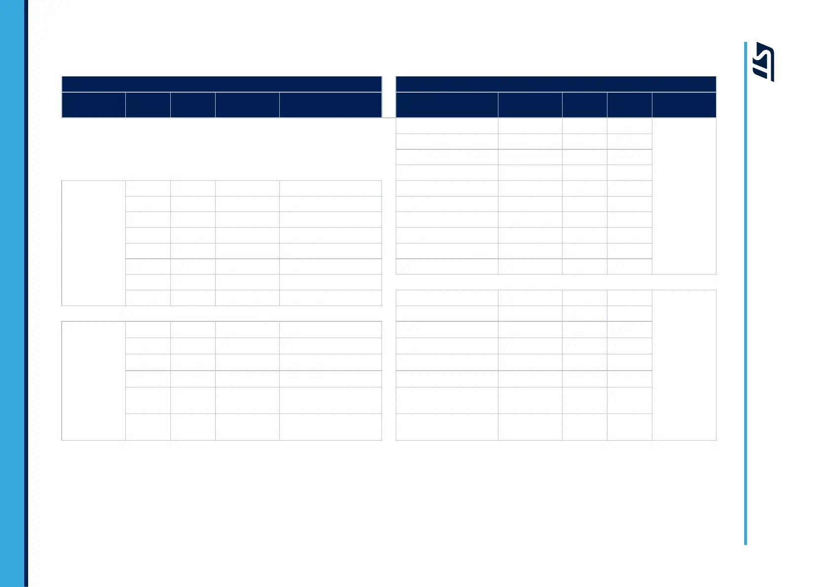
Table 16. ARDUINO
®
Uno V3 connectors pinout
Left connectors Right connectors
Connector Pin
number
Pin name MCU pin SoC function
SoC function MCU pin Pin name Pin
number
Connector
I2/3C1_SCL PH9 D15 10
CN12 Digital
I2/3C1_SDA PC1 D14 9
AVDD - AREF 8
Ground - GND 7
CN8 Power
1 - - 5V_IN test
SPI5_SCK PE15 D13 6
2 IOREF - 3.3 V ref
SPI5_MISO PH8 D12 5
3 RESET NRST RESET
TIM14_CH1 or SPI5_MOSI PG2 D11 4
4 +3V3 - 3.3 V output
TIM16_CH1 or SPI_CS PA3 D10 3
5 +5V - 5 V output
TIM1_CH4 PE14 D9 2
6 GND - Ground
- PE7 D8 1
7 GND - Ground
8 VIN - Power input
- PD6 D7 8
CN11 Digital
TIM1_CH3 PE13 D6 7
CN7 Analog
1 A0
PA5 or PD7
(1)
ADC12_INP18(PA5)
TIM1_CH2N PE10 D5 6
2 A1
PA9 or PC10
(1)
ADC12_INP10(PA9)
-
PH5 D4 5
3 A2
PA10 or PE12
(1)
ADC12_INP11(PA10)
TIM1_CH1 PE9 D3 4
4 A3
PA12 or PD11
(1)
ADC12_INP13(PA12)
-
PD0 D2 3
5 A4
PF3/PC12
(1)
or
PC1
(2)
ADC12_INP16(PF3) or
I2C1_SDA(PC1)
USART2_TX PD5 D1 2
6 A5
PB10/PH2
(1)
or
PH9
(2)
ADC12_INP8(PB10) or
I2C1_SCL(PH9)
USART2_RX PF6 D0 1
1. Since for ADC, the level of MCU pins is 1.8 V, while for digital I/Os the level of MCU pins is 3.3 V.
2. By default, the I2C1 function is disabled with the configuration: SB32 and SB34 OFF, SB31 and SB33 ON. To get the I2C1 function, the configuration must be: SB32 and SB34 ON,
SB31 and SB33 OFF.
UM3300
- Rev 1
page 26/49
UM3300
Board connectors