7 Hardware layout and configuration
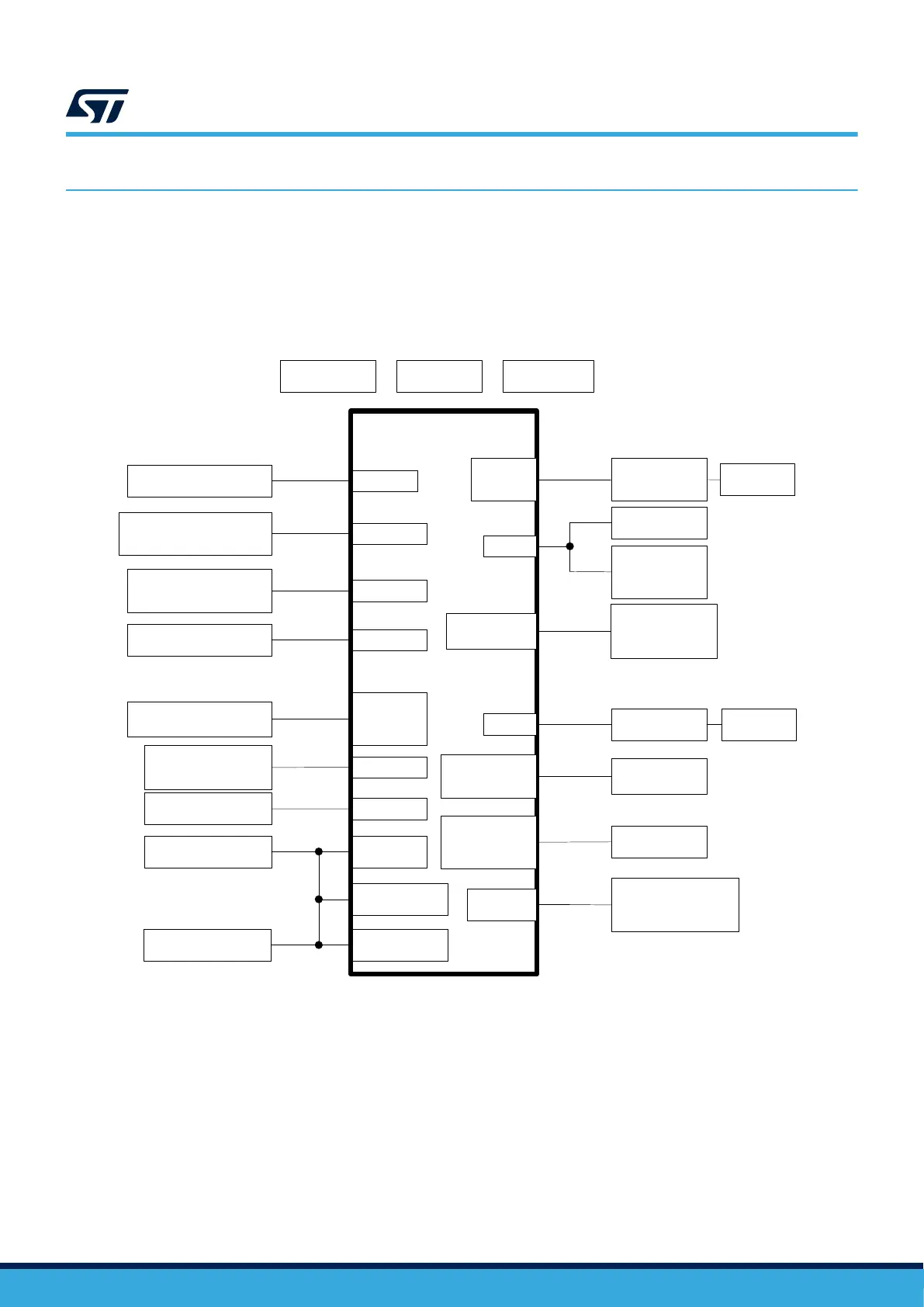
The STM32N6570-DK Discovery kit is designed around the STM32N657X0H3Q microcontroller, in VFBGA264
package. The hardware block diagram in Figure 3 illustrates the connection between the microcontroller and the
peripherals. Figure 4 and Figure 5 help to locate these features on the STM32N6570-DK Discovery board.
7.1 Hardware block diagram and board layout
Figure 3.
Hardware block diagram
DT59548V1
STM32N657X0H3Q
LSE/HSE
SWD and
JTAG
32 KHz crystal
48 MHz crystal
STLINK-V3EC
MDF
SAI1 and
I2C2
Two LEDs
User, tamper and
reset buttons
microSD
TM
card
PHY
RGMII
SDMMC2
USB Type-A
USB2
XSPIM_P2
Octo-SPI flash memory
VCP
USART1
3.3 V power
supply
1.8 V power
supply
RGB, GPIOs,
and I2C2
TFT LCD with
touch panel
(MB1860)
STMod+
connector
XSPIM_P1
Hexadeca-SPI PSRAM
CSI,
GPIOs
and I2C1
Camera module
connector
ARDUINO
®
connector
SMPS power
supply
Codec
Headset
connector
MEMs
microphone
MEMs
connector
(MB1671)
USB Type-C
®
source and sink
USB1
RJ45
connector
GPIOs, I2C1,
ADCs and
SPI5
GPIOs, I2C1,
USART2, ADC
and SPI5
GPIOs
TraceMIPI20
UM3300
Hardware layout and configuration
UM3300 - Rev 1
page 8/49