Chapter 2: Installation
2-29
BIOS LICENSE
IPMI CODE
MAC CODE
BAR CODE
DESIGNED IN USA
1.01Rev:
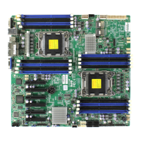
X10SRL-F
1
+
LAN
CTRL
LAN
CTRL
BMC
JP3
JTPM1
JF1
JD1
T-SGPIO1
T-SGPIO2
T-SGPIO3
JOH1
JL1
JPME2
JWD1
JPG1
JPB1
JI2C2
JI2C1
JBR1
JPL2
JPL1
JVR1
JSD1
JSD2
JIPMB1
JPWR1
UID LED - LE1
LE2
LEDM1
JBT1
BT1
FAN4
FAN1
FAN2
FAN3
FANA
FAN5
J24
JPI2C1
JSTBY1
S-SATA3
I_SATA4
I-SATA0
I-SATA1I-SATA2
I-SATA3
S-SATA0
S-SATA1
S-SATA2
I-SATA5
SP1
CPU
CPU SLOT5 PCI-E 3.0 X8
CPU SLOT4 PCI-E 3.0 X8(IN X16)
USB0/1
DIMMC2
USB8/9
USB6/7
USB2/3(3.0)
LAN1
DIMMA2
DIMMA1
USB10(3.0)
LAN2
USB4/5
CPU SLOT2 PCI-E 3.0 X4(IN X8)
PCH SLOT1 PCI-E 2.0 X4(IN X8)
COM2
COM1
DIMMB2
DIMMB1
DIMMD2
DIMMD1
IPMI_LAN
UID - SW
5V STBY
USB11(3.0)
IPMI
VGA
CPU SLOT7 PCI-E 3.0 X8
DIMMC1
CPU SLOT3 PCI-E 3.0 X4(IN X8)
CPU SLOT6 PCI-E 3.0 X8(IN X16)
Intel PCH
1
1
A. DOM PWR 1
B. DOM PWR 2
C. Standby PWR
A
B
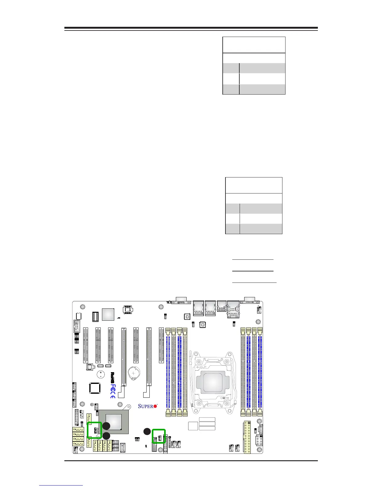
DOM PWR Connector (JSD1)
The Disk-On-Module (DOM) power
connectors, located at JSD1 and
JSD2, provide 5V power to a solid
state DOM storage device connected
to one of the SATA ports. See the table
on the right for pin denitions.
DOM PWR
Pin Denitions
Pin# Denition
1 5V
2 Ground
3 Ground
Standby Power
The Standby Power header is located
at JSTBY1 on the motherboard. See
the layout below for the location.
Standby Power
Pin Denitions
Pin# Denition
1 +5V Standby
2 Ground
3 No Connection
C
 Loading...