7-4
Rev 2.2, 10/31/94
7.3 Block Diagrams
On the preceding and following pages, you can find the block diagrams for the de-esser,
dynamic noise reduction, dynamics processors, delay processor, and the entire 601. Please take
a moment and take note of the following:
7.3.1 Overall Block Diagram
Refer to Figure 7-2.
r
Two DSP chips handle all of the signal processing functions.
r
The AES/EBU or S/PDIF inputs and outputs may be re-configured to connect between the
DSP section and the D/A converter.
r
The external digital inputs may also be used for an external clock reference.
r
Presets and global parameters are stored in battery backed-up RAM.
r
Both audio channels are always processed together. It is not possible to separate the two
channels.
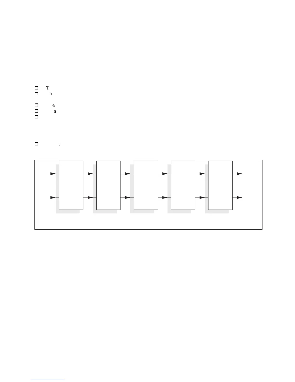
7.3.2 Sequence of Processing
r
Note the order of the different signal processors.
7.3.3 Dynamics Block
❑ The compressor and expander operate simultaneously. The gain reduction value is
determined by the processor having the greatest gain-reduction output.
❑ The auto release circuitry operates when the AGC/Leveler is engaged.
❑ The signal path delay compensates for the computational time needed to compute the
gain-reduction amount. For extremely short attack times, you may need to increase this
parameter to allow the compressor to anticipate the input signal.
❑ Both channels always receive the same gain-reduction signal and the larger of the two
input signals at any given instant becomes the source for any gain-reduction
computations.
❑ The MIDI edit buffer parameter numbers are shown in parenthesis.
Software
Generated
DE-ESS
Circuitry
Software
Generated
Dynamic
Noise
Reduction
Circuitry
Software
Generated
Parametric
Filter
Circuitry
Software
Generated
Dynamics
Processor
Circuitry
Software
Generated
Delay
Circuitry
Input 1 Output 1
Input 2
Output 2
Figure 7-3. Sequence of Processing.