TB8100 Installation and Operation Manual Circuit Description 15
© Tait Electronics Limited June 2005
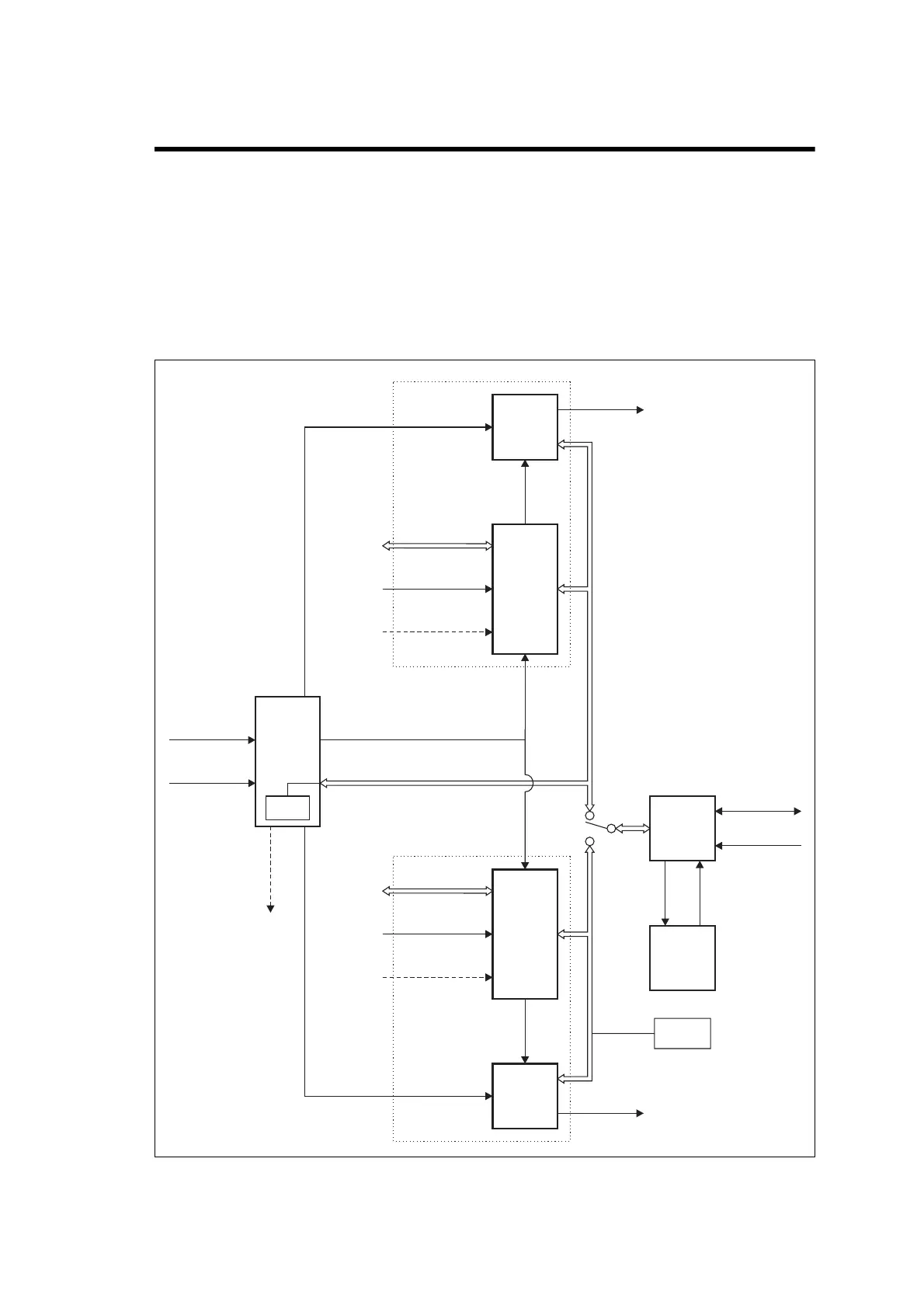
2 Circuit Description
Figure 2.1 below shows a typical TB8100 dual base station system of 5W or
50W. It illustrates the main inputs and outputs for power, RF and control
signals, as well as the interconnection between modules. The circuitry of
the individual modules that make up the BSS is described in more detail in
the following sections.
Figure 2.1 Dual base station system high level block diagram
Reciter 2
Reciter 1
PMU
PA 2
PA 1
System Control Bus
RF From
Antenna
Base Station 2
*located on subrack
interconnect board
Base Station 1
RF To
Antenna
RF To
Antenna
System I/O
External Reference
Frequency
(if used)
(if used)
RF From
Antenna
System I/O
External Reference
Frequency
AC I/P
DC I/P
28VDC
(low current)
Control
Panel
Cooling
Fans
Microphone I/P
Rotation
Sensor
RS-232
DC
RF +
PA Key
RF +
PA Key
Auxiliary
DC O/P
(Optional)
28VDC
(high current)
28VDC
(high current)
I C Current
Source
2
I C Current
Source*
2

 Loading...


