2205 Service
LIST OF ILLUSTRATIONS
Figure
Page
1-1
1-2
2-1
2-2
2-3
2-4
2 - 5
3 - 1
3-2
3-3
3-4
3-5
3-6
5-1
6-1
9-1
9-2
9-3
9-4
9-5
9-6
9-7
9-8
9-9
9-10
9-11
9-12
9-13
9-14
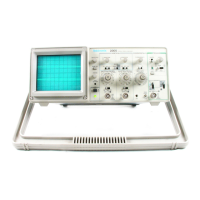
The 2205 Oscilloscope
viii
Maximum input voltage vs frequency derating curve for CH 1 OR X, CH 2 or Y, and
EXT INPUT or Z conn ecto rs.....................................................................................
..
........
Instrument dimensional d raw in g
................................
............................................
..
Voltage Selector switch, fuse, power-cord receptacle, and plastic clamp .
Front panel controls, connectors, and indica tors
................................
Rear Panel ............ ..
.................................................... ......................................
Graticule measurement m arkings.....................................................................
Probe compensation
.
.
..
..
..
.......................................... ....................
..
.
............
..
Block diagram of the Channel 1 Attenuator
.
....................................
Block diagram of the Channel S w itching
..............
.
..........................
Block diagram of the Sweep Generator and Logic
.
..........................
Block diagram of the Horizontal A m plifie r
................
........................
Simplified diagram of the DC Restorer
....................
........................
Block diagram of the Power S upply...................................................
Attenuator trim m er adjustm ents
..............................
.
........
2-2
........
2-4
........
2-6
........
2-7
........
2-9
........
3-3
........
3-5
........
3-9
-----
3-11
•... 3-13
-----
3-15
........
5-8
M ulti-connector holder orie nta tio n
........................
......................
................
.
..
..
Color codes for resistors.
Semiconductor lead configurations*
Locating components on schematic diagrams and circuit board illustrations.
Block diagram.
Component view of A3—Front Panel board.
Circuit view of A3—Front Panel board.
A2—Timebase/Attenuator board.
A1—Main board component view.
Circuit view of A1—Main board.
A4—Mains Input board.
Adjustment locations of A1—Main board component view.
Adjustment locations of A1—Main board circuit view.
A2—Timebase/Attenuator board adjustment locations.
A3—Front Panel board adjustment location.