3-77
During the periods that capacitor C is charging and
discharging, the control grid voltage is held stable by the
long-time-constant discharge path of capacitor D through
resistor F. Any charge removed from capacitor D during
the positive transitions of the ac waveform will be replaced
on the negative transitions.
As the INTENSITY control is advanced, the amplitude
of the square-wave Z-Axis signal increases accordingly.
This increased signal amplitude decreases the difference
between the upper and lower clamped levels of the ac
waveform, and less charge is added to capacitor D. The
decreased voltage across capacitor D decreases the
potential difference between the control grid and the
cathode, and more crt beam current is present. Increased
beam current increases the crt display intensity,
The potential difference between the control grid and
the cathode controls electron-beam current (the display
lntensity). With no Z-Axis signal applied (INTENSITY con-
trol off), capacitor D will be charged to its maximum nega-
tive value since the difference between the two clamped
voltage levels is at its maximum value. This is the
minimum intensity condition and reflects the setting of the
Grid Bias potentiometer. During calibration, the Grid Bias
pot is adjusted so that the difference between the upper
clamping level (set by the Grid Bias pot) and the "no sig-
nal" level of the Z-Axis drive signal (VZ) produces a con-
trol grid bias that barely shuts off the crt electron beam.
When the ac waveform begins its transition from the
upper clamped level back to the lower clamped level, diode
A becomes reverse biased. Diode B becomes forward
biased, and an additional charge proportional to the nega-
tive excursion of the ac waveform (difference between the
upper clamped level and the lower clamped level) is added
to capacitor D through diode B and resistor G. The
amount of charge added to capacitor D depends on the
setting of the front-panel INTENSITY control, as it sets the
lower clamping level of the ac waveform. This added
charge determines the potential of the control grid with
respect to the crt cathode.
When the ac waveform applied to pin 15 begins its
transition from the lower clamped level (set by the Z-Axis
signal) towards the upper clamped level (set by the Grid
Bias potentiometer), the charge on capacitor C increases.
The additional charge is proportional to the voltage
difference between the two clamped voltage levels.
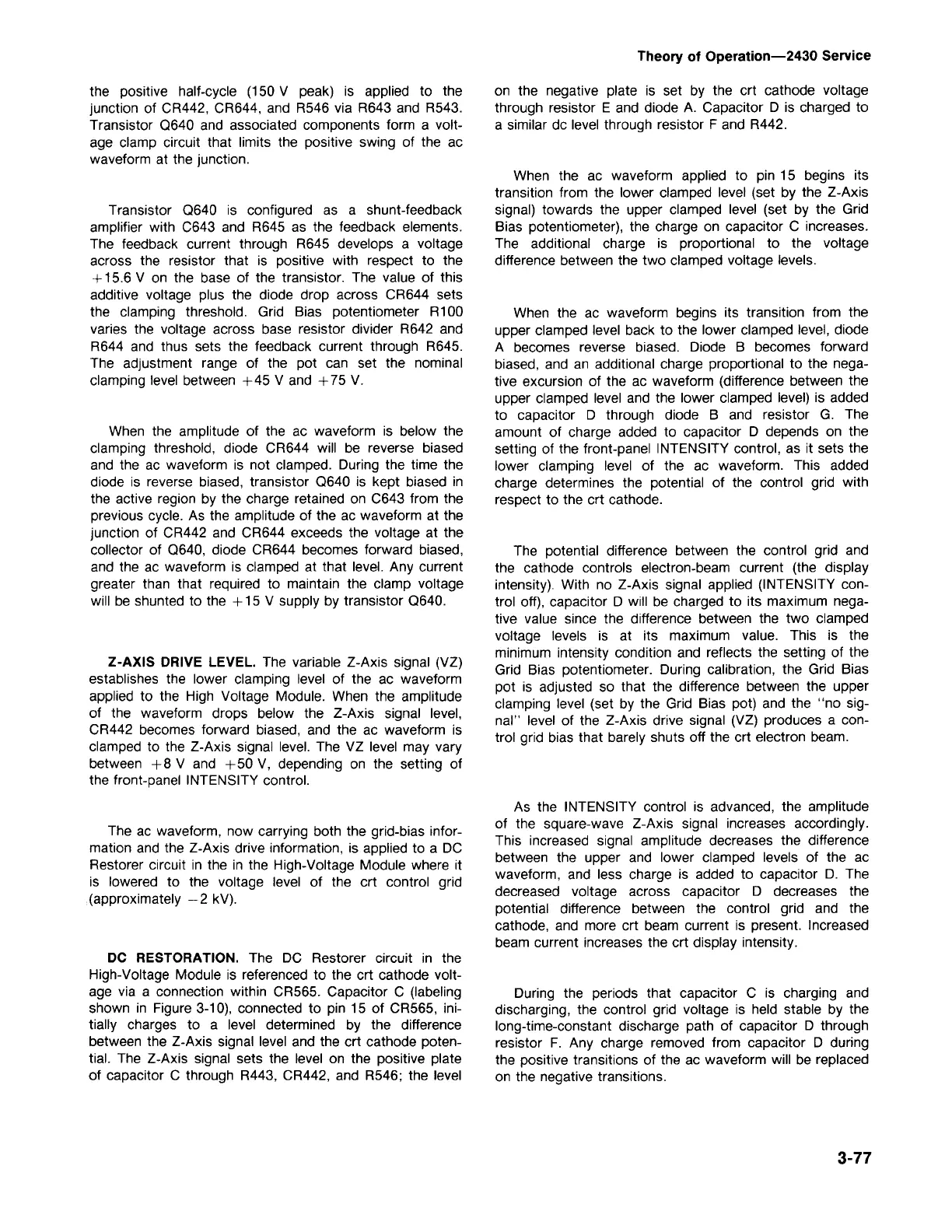
on the negative plate is set by the crt cathode voltage
through resistor E and diode A. Capacitor D is charged to
a similar dc level through resistor F and R442.
Theory of Operation-2430 Service
DC RESTORATION. The DC Restorer circuit in the
High-Voltage Module is referenced to the crt cathode volt-
age via a connection within CR565. Capacitor C (labeling
shown in Figure 3-10), connected to pin 15 of CR565, ini-
tially charges to a level determined by the difference
between the Z-Axis signal level and the crt cathode poten-
tial. The Z-Axis signal sets the level on the positive plate
of capacitor C through R443, CR442, and R546; the level
The ac waveform, now carrying both the grid-bias infor-
mation and the Z-Axis drive information, is applied to a DC
Restorer circuit in the in the High-Voltage Module where it
is lowered to the voltage level of the crt control grid
(approximately -2 kV).
Z-AXIS DRIVE LEVEL. The variable Z-Axis signal (VZ)
establishes the lower clamping level of the ac waveform
applied to the High Voltage Module. When the amplitude
of the waveform drops below the Z-Axis signal level,
CR442 becomes forward biased, and the ac waveform is
clamped to the Z-Axis signal level. The VZ level may vary
between + 8 V and + 50 V, depending on the setting of
the front-panel INTENSITY control.
When the amplitude of the ac waveform is below the
clamping threshold, diode CR644 will be reverse biased
and the ac waveform is not clamped. During the time the
diode is reverse biased, transistor 0640 is kept biased in
the active region by the charge retained on C643 from the
previous cycle. As the amplitude of the ac waveform at the
junction of CR442 and CR644 exceeds the voltage at the
collector of 0640, diode CR644 becomes forward biased,
and the ac waveform is clamped at that level. Any current
greater than that required to maintain the clamp voltage
will be shunted to the + 15 V supply by transistor 0640.
Transistor 0640 is configured as a shunt-feedback
amplifier with C643 and R645 as the feedback elements.
The feedback current through R645 develops a voltage
across the resistor that is positive with respect to the
+ 15.6 V on the base of the transistor. The value of this
additive voltage plus the diode drop across CR644 sets
the clamping threshold. Grid Bias potentiometer R100
varies the voltage across base resistor divider R642 and
R644 and thus sets the feedback current through R645.
The adjustment range of the pot can set the nominal
clamping level between +45 V and + 75 V.
the positive half-cycle (150 V peak) is applied to the
junction of CR442, CR644, and R546 via R643 and R543.
Transistor 0640 and associated components form a volt-
age clamp circuit that limits the positive swing of the ac
waveform at the junction.