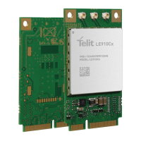
LE910Cx mPCIe Hardware Design Guide
1VV0301510 Rev. 13 Page 23 of 73 2021-07-07
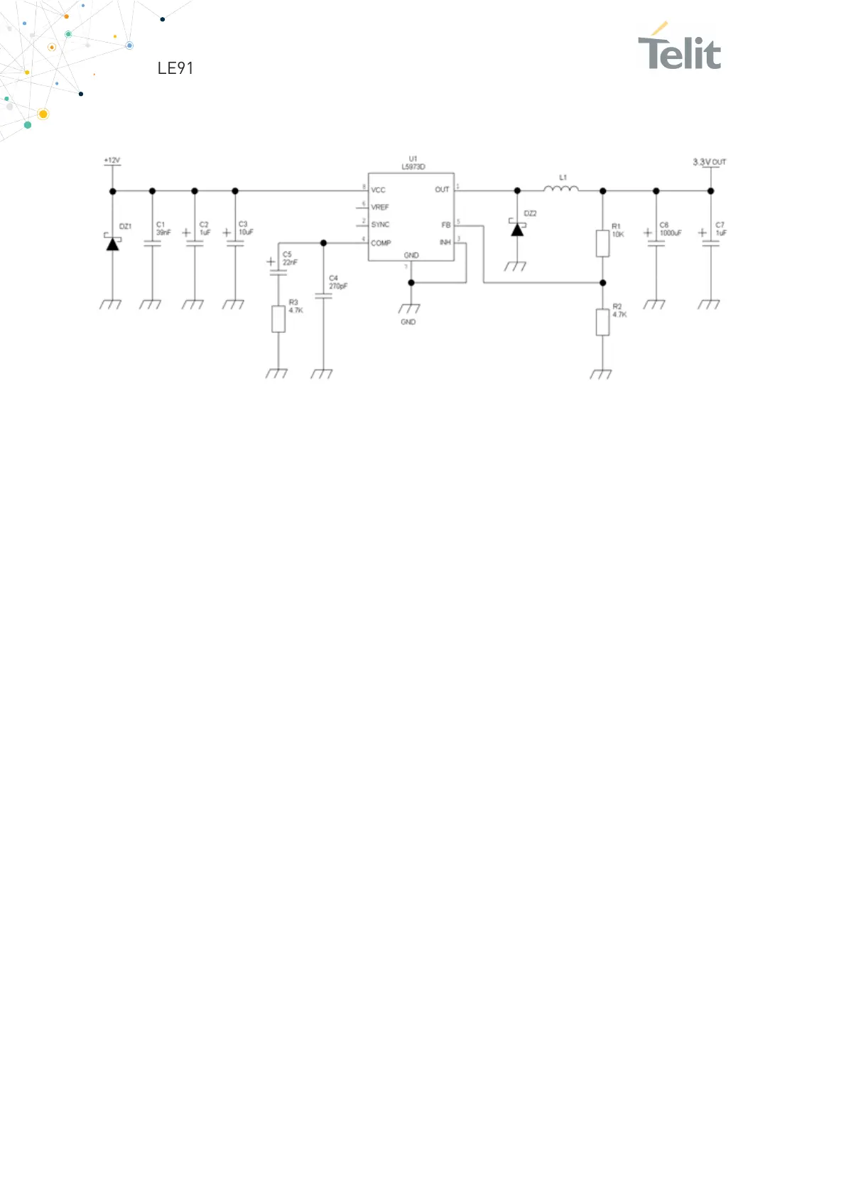
An example of switching regulator with 12V input is in the below schematic:
Figure 2: An Example of Switching Regulator with 12V Input
4.3.2. Thermal Design Guidelines
The thermal design of the application board and the power supply heat sink should be
done with the following specifications:
• Typical average current consumption during xE910Cx Mini PCIe transmission @
Max PWR level at min battery level (LTE) : 700 mA
• Average current during idle (USB enabled): 30 mA
• Average current during idle (USB disabled): 5 mA
• Average current during airplane mode (USB disabled): 2 mA
Considering the very low current during Idle, especially if the Power Saving function is
enabled, it is possible to consider from the thermal point of view that the device absorbs
significant current mainly during the Data session. In LTE/WCDMA/HSPA mode, the
xE910Cx Mini PCIe emits RF signals continuously during transmission. Therefore, special
attention must be pain to how to dissipate the heat generated.
The LE910Cx mPCIe card is designed to conduct the heat flow from the module IC’s
towards the bottom of the mPCIe PCB across GND metal layers
For best performance, the application board’s copper layers should be used to dissipate
heat out of the mPCIe card.
In order to ensure proper thermal flow from the mPCIe card to the application board, the
mPCIe card bottom side should be thermally connected to the application board top side
via proper thermal pad.
 Loading...