www.ti.com
BP-ADS7128EVM Overview
5
SBAU331–May 2019
Submit Documentation Feedback
Copyright © 2019, Texas Instruments Incorporated
BP-ADS7128 BoosterPack™ Plug-In Module
2.1 Connector for Channels
The BP-ADS7128 is designed for easy interface to an external, analog single-ended source, or to GPIOs
through a 100-mil header. Connector J5 provides a connection to the device channels. Table 1 lists the
channel connections. The ADS7128 channel AIN0 has a buffered operational amplifier, TLV9061, to drive
the analog input. Channels AIN1 through AIN6 have a resistor and capacitor filter circuit to condition the
analog input. GPIO7 does not have a resistor and capacitor filter used for the single-ended analog input;
instead, GPIO7 has a resistor and light-emitting diode (LED) to visibly demonstrate and monitor the
channel state.
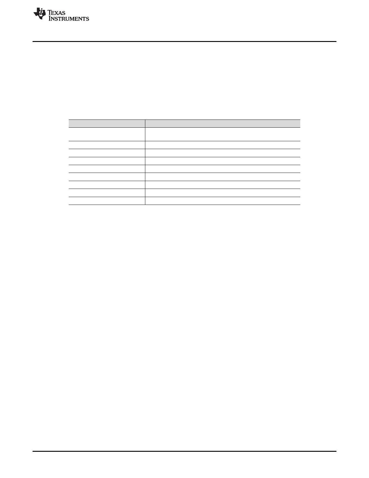
Table 1. Channel Connections
J5 Connector Pin Description
J5:1
Single-ended analog input with buffer or GPIO for channel 0 of the
ADC
J5:2 Single-ended analog input or GPIO for channel 1 of the ADC
J5:5 Single-ended analog input or GPIO for channel 2 of the ADC
J5:6 Single-ended analog input or GPIO for channel 3 of the ADC
J5:7 Single-ended analog input or GPIO for channel 4 of the ADC
J5:8 Single-ended analog input or GPIO for channel 5 of the ADC
J5:11 Single-ended analog input or GPIO for channel 6 of the ADC
J5:12 Single-ended analog input or LED GPIO for channel 7 of the ADC
J5:3 and J5:4; J5:9 and J5:10 BoosterPack™ ground
2.2 Digital Interface
As noted in Section 1, the BP-ADS7128 interfaces with the MSP-EXP432E401Y LaunchPad™, which in
turn communicates with the computer over the USB. The two devices on the booster pack that the
MSP432E401Y communicates over I
2
C are the ADS7128 ADC and the electrically erasable programmable
read-only memory (EEPROM). The EEPROM comes preprogrammed with the information required to
configure and initialize the BP-ADS7128 platform. Once the hardware is initialized, the EEPROM is no
longer used.
2.3 ADS7128 LaunchPad™ Interface
The BP-ADS7128 supports the I
2
C digital interface and functional modes as detailed in the ADS7128
device datasheet. The MSP432E401Y LaunchPad™ is capable of operating at a 3.3-V logic level and is
directly connected to the digital I/O lines of the ADC.
2.4 Power Supplies
The device supports a wide range of operation on its analog supply. The AVDD can operate from 2.35 V
to 5.5 V. The DVDD operates from 1.65 V to 5.5 V, independent of the AVDD supply. The 3.3-V voltage
regulator available on the MSP-EXP432E401Y is used to supply 3.3 V to DVDD and to AVDD through a
low-dropout (LDO) regulator, the TPS78001, on the BP-ADS7128. There is an onboard option to use an
external power supply for DVDD.
 Loading...


