ADCSOCAO
ADCSOCBO
or
t
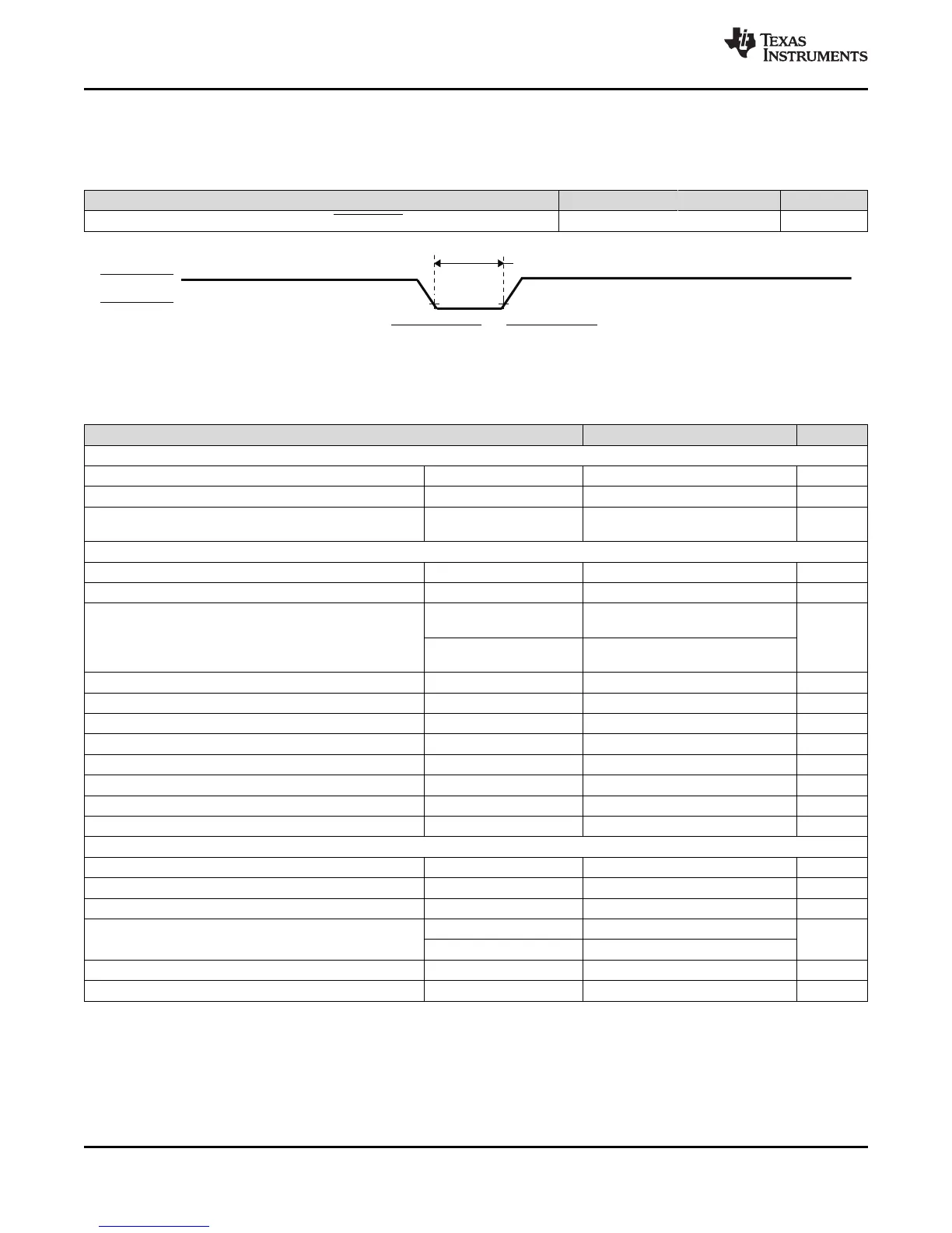
w(ADCSOCL)
86
TMS320F28069
,
TMS320F28068
,
TMS320F28067
,
TMS320F28066
TMS320F28065, TMS320F28064, TMS320F28063, TMS320F28062
SPRS698F –NOVEMBER 2010–REVISED MARCH 2016
www.ti.com
Submit Documentation Feedback
Product Folder Links: TMS320F28069 TMS320F28068 TMS320F28067 TMS320F28066 TMS320F28065
TMS320F28064 TMS320F28063 TMS320F28062
Detailed Description Copyright © 2010–2016, Texas Instruments Incorporated
6.9.2.1.2 ADC Start-of-Conversion Electrical Data/Timing
Table 6-26. External ADC Start-of-Conversion Switching Characteristics
over recommended operating conditions (unless otherwise noted)
PARAMETER MIN MAX UNIT
t
w(ADCSOCL)
Pulse duration, ADCSOCxO low 32t
c(HCO)
cycles
(1) INL will degrade when the ADC input voltage goes above V
DDA
.
(2) 1 LSB has the weighted value of full-scale range (FSR)/4096. FSR is 3.3 V with internal reference and V
REFHI
- V
REFLO
for external
reference.
(3) For more details, see the TMS320F28069, TMS320F28068, TMS320F28067, TMS320F28066, TMS320F28065, TMS320F28064,
TMS320F28063, TMS320F28062 Piccolo MCUs Silicon Errata (SPRZ342).
(4) Periodic self-recalibration will remove system-level and temperature dependencies on the ADC zero offset error.
(5) V
REFLO
is always connected to V
SSA
on the 80-pin PN and PFP devices.
(6) V
REFHI
must not exceed V
DDA
when using either internal or external reference modes. Since V
REFHI
is tied to ADCINA0 on the 80-pin PN
and PFP devices, the input signal on ADCINA0 must not exceed V
DDA
.
Figure 6-22. ADCSOCAO or ADCSOCBO Timing
6.9.2.1.3 On-Chip Analog-to-Digital Converter (ADC) Electrical Data/Timing
Table 6-27. ADC Electrical Characteristics
PARAMETER MIN TYP MAX UNIT
DC SPECIFICATIONS
Resolution 12 Bits
ADC clock 90-MHz device 0.001 45 MHz
Sample Window 7 64
ADC
Clocks
ACCURACY
INL (Integral nonlinearity)
(1)
–4 4 LSB
DNL (Differential nonlinearity), no missing codes –1 1.5 LSB
Offset error
(2)
Executing a single self-
recalibration
(3)
–20 20
LSB
Executing periodic self-
recalibration
(4)
–4 4
Overall gain error with internal reference –60 60 LSB
Overall gain error with external reference –40 40 LSB
Channel-to-channel offset variation –4 4 LSB
Channel-to-channel gain variation –4 4 LSB
ADC temperature coefficient with internal reference –50 ppm/°C
ADC temperature coefficient with external reference –20 ppm/°C
V
REFLO
–100 µA
V
REFHI
100 µA
ANALOG INPUT
Analog input voltage with internal reference 0 3.3 V
Analog input voltage with external reference V
REFLO
V
REFHI
V
V
REFLO
input voltage
(5)
V
SSA
0.66 V
V
REFHI
input voltage
(6)
2.64 V
DDA
V
with V
REFLO
= V
SSA
1.98 V
DDA
Input capacitance 5 pF
Input leakage current ±2 μA