The interfaces on the alternative functions are not described in this document since they differ
between the modules. Information related to these functions can be found in the datasheets of the
modules.
2.1.3 Pin Numbering
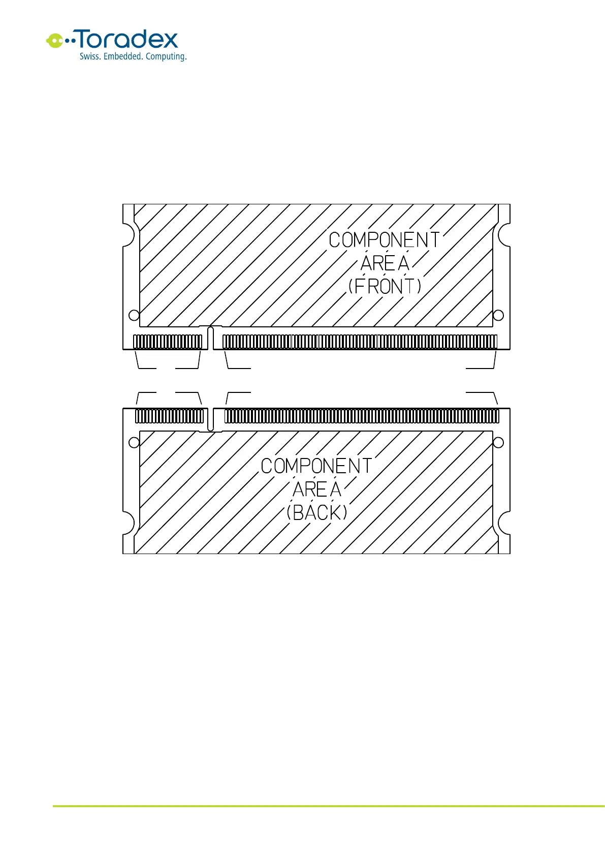
The diagrams in the figures below show the pin numbering schema on both sides of the module.
The schema is equal to the JEDEC MO-224 DDR SO-DIMM standard. The odd pin numbers are
located on the top side of the module.
Figure 1: Colibri Module Pin Numbering Schema
2.1.4 Pin Reset State
The datasheets of the Colibri module provide information about the default reset status of the IO
pins. Please be aware that the pin reset status is only guaranteed during the release of the reset
signal. Some of the modules switch the IO bank voltages to follow the power-up sequence of the
SoC. This means the IO pins can have an undefined state between applying the main power to the
module until the nRESET_OUT is released. For carrier board designs that do not allow undefined
pin states, it is recommended to ensure that the peripheral devices are not powered before the
nRESET_OUT is released. Another solution can be gating the related IO signals with the
nRESET_OUT signal.