4.5 JTAG Test Pads
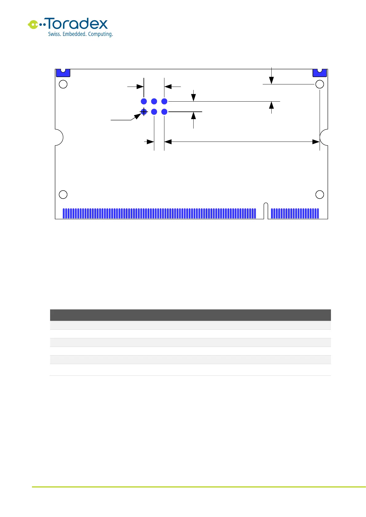
Figure 62: Location of JTAG Test Pads (bottom view, dimensions in mm)
The JTAG interface is not generally required for software development with the Colibri module.
There is always the possibility of reprogramming the module using the Recovery Mode over USB or
UART. However, for debugging the operating system, especially for real-time operating systems, it
might be beneficial having access to the JTAG interface of the SoC.
The JTAG interface is located on test points on the underside of the module. The location is the
same for all modules in the Colibri family. There are a total of six test pads, of which five are used
for the JTAG interface. The sixth test pad is used for module testing and should be left unconnected
on the carrier board. Please note the unusual pin numbering.
Table 29: JTAG Signals
Please pay attention to the interface voltage. Depending on the module, the IO voltage can be
3.3V or 1.8V. It is crucial to use the correct JTAG interface voltage. Carefully read the module
datasheet for more information. On the Colibri Evaluation Board version 3.1 and later, there is a
jumper for setting the JTAG IO voltage (JP29).