RF Output
Circuit Descriptions
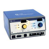
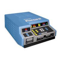
Force 2 Service Manual 5-7
stretcher shuts down the supply's control IC for about 1/3 of a second and
then soft starts the supply. The R-C network on the 3526 pin 7 provides a
power on reset.
A separate switching power supply on the rear of the chassis supplies the
low voltages. It supplies regulated +5Vdc, +12Vdc, and -12Vdc to the
Power Supply board where all voltages filter with 10 µF capacitors. The
-12Vdc voltage converts to -5Vdc using a LM336 regulator. The supply
voltages transfer to the Interface board and Monopolar Control/Display
board through the 40-pin ribbon cable.
RF Output
This circuitry resides on the Power Supply board and amplifies the CPU
signal T-on, RFT (0) to the level the front panel power setpoint requires.
T-off, RFT (1) is not a requirement and therefore terminates at the ribbon
cable with a 10k ohm resistor. Current limiting and peak voltage limiting
circuits prevent damage under extreme load conditions. Varying the
supply voltage controls the power. Both DC supply and RF current limit
levels calibrate for each mode - cut, coag, blend and bipolar. The output
tuning and transformer turns ratio is different for cut and coag waveforms
and a relay performs the selection. Eight power FETs act as RF switching
elements. A current sampling resistor at the sources provides input to a
current limit circuit. Gate drive is direct at a 12V level. The drains have
diodes in series to allow the output transformer primary voltage to swing
negative in coag. The cut waveform drive is at a 50% duty cycle with a
1 µs ON time. Turning on the FETs for 2 µs every 32 µs generates the coag
drive waveform.
RF control uses a RS flip-flop to control the T-on pulse to the output stage.
The RS flip-flop can be reset by feedback circuits to reduce output drive
pulses for control of RF output. Excessive output current compared to
ICON or excessive negative going voltage compared to the ECON setting
can generate this pulse reduction, pulse wacking.
Comparing output transformer primary voltage to ECON controls the RF
leakage and high impedance power. The signal from the primary
attenuates and then compares to a reference level proportional to the
ECON setting. This attenuation is mode specific for cut, blend, and coag.
When the negative going voltage from the primary exceeds the reference
level, this removes (wacks) the RF drive pulses and adds a resistive load in
parallel to the primary to dampen the output waveform.
The CPU supplies the current limit reference, ICON, and varies as the
square root of power with an offset at low powers. When peak voltage
limiting occurs, the reference voltage to the LM306 current limit com-
parator reduces which in turn reduces the output pulse width. At high
Warning
The power FETs and other components on the supply heatsink are at line
potential. Use extreme caution when probing this circuitry.