18 www.xilinx.com AC701 Evaluation Board
UG952 (v1.3) April 7, 2015
Chapter 1: AC701 Evaluation Board Features
The AC701 board DDR3 memory interface adheres to the constraints guidelines
documented in the DDR3 Design Guidelines section of the 7
Series FPGAs Memory Interface
Solutions User
Guide (UG586) [Ref 3]. The AC701 board DDR3 memory interface is a 40 Ω
impedance implementation. Other memory interface details are available in the
7
Series FPGAs Memory Interface Solutions User Guide (UG586) and the 7 Series FPGAs
Memory Resources User
Guide (UG473) [Ref 4]. For more DDR3 SODIMM details, see the
Micron MT8JTF12864HZ-1G6G1 data sheet [Ref 15].
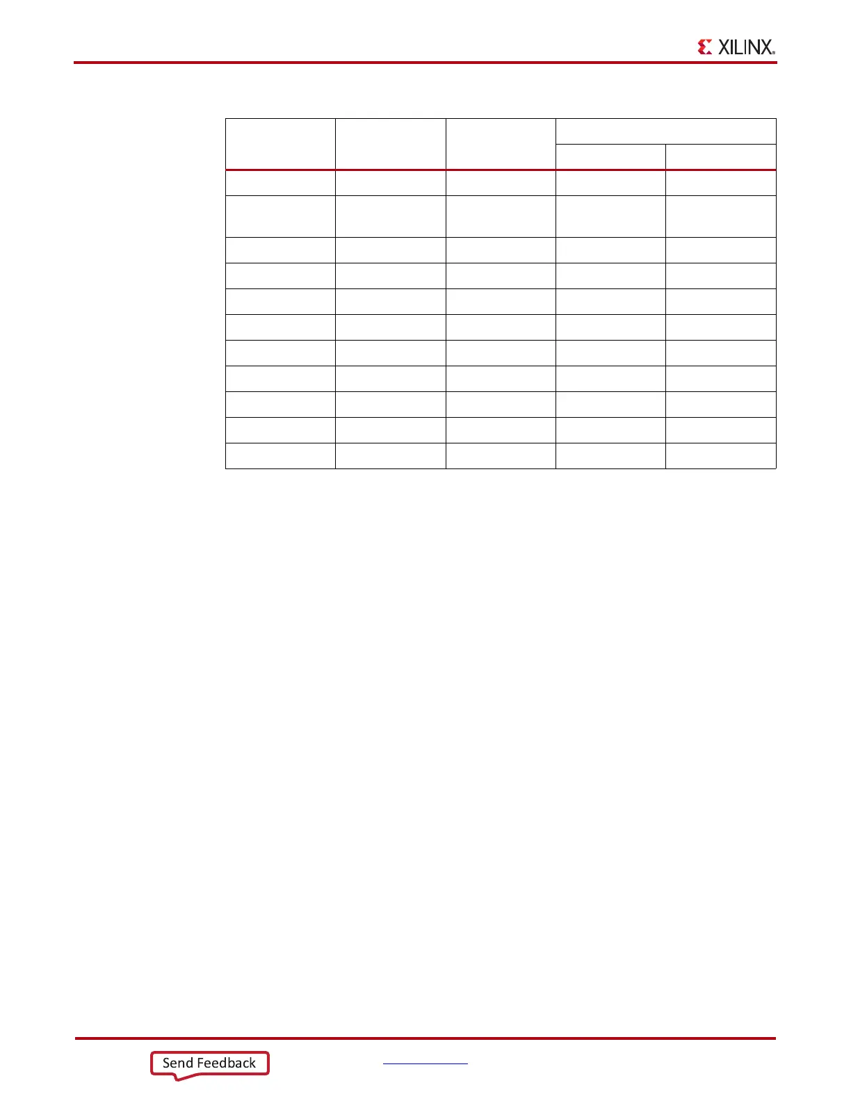
T2 DDR3_S1_B SSTL15 121 S1_B
U1
DDR3_TEMP_
EVENT
LVCMOS15 198 EVENT_B
R1 DDR3_WE_B SSTL15 113 WE_B
T4 DDR3_CAS_B SSTL15 115 CAS_B
P1 DDR3_RAS_B SSTL15 110 RAS_B
P4 DDR3_CKE0 SSTL15 73 CKE0
N4 DDR3_CKE1 SSTL15 74 CKE1
L2 DDR3_CLK0_N DIFF_SSTL15 103 CK0_N
M2 DDR3_CLK0_P DIFF_SSTL15 101 CK0_P
N2 DDR3_CLK1_N DIFF_SSTL15 104 CK1_N
N3 DDR3_CLK1_P DIFF_SSTL15 102 CK1_P
Table 1-4: DDR3 Memory Connections to the FPGA (Cont’d)
FPGA Pin (U1)
Schematic Net
Name
I/O Standard
J1 DDR3 Memory
Pin Number Pin Name