AC701 Evaluation Board www.xilinx.com 25
UG952 (v1.3) April 7, 2015
Feature Descriptions
System Clock Source
[Figure 1-2, callout 6]
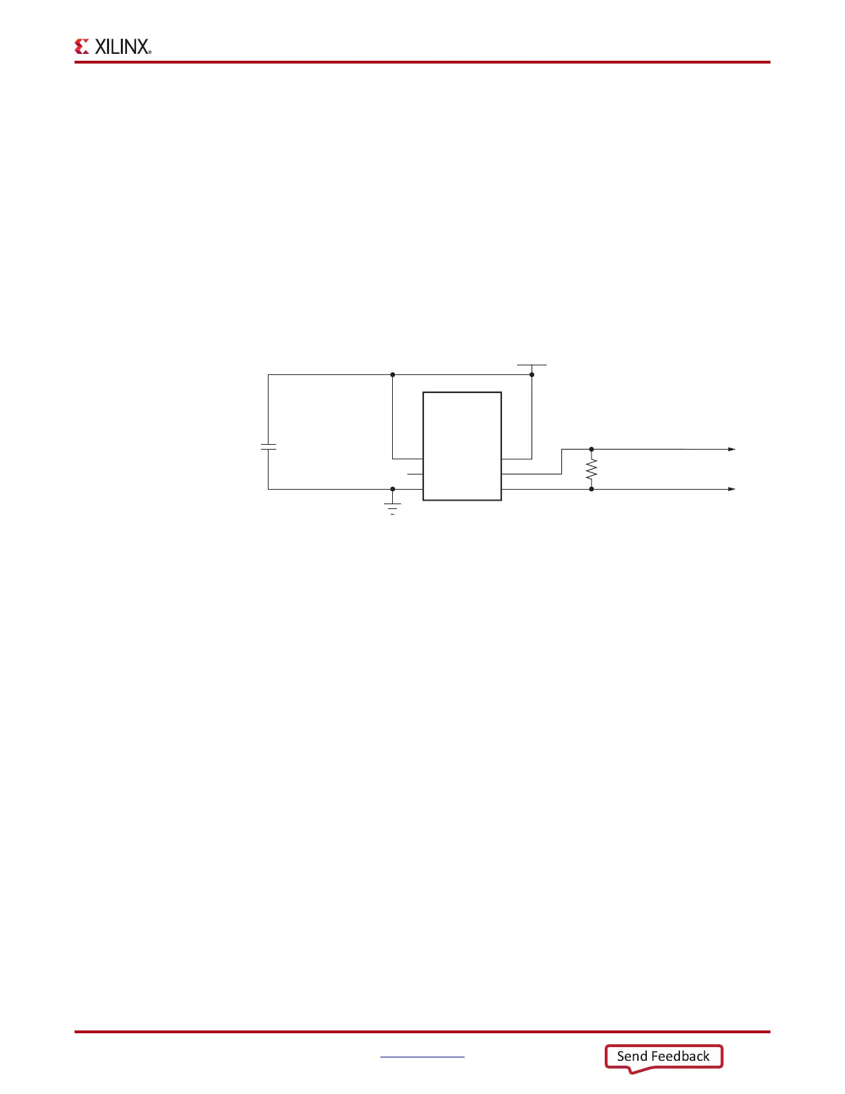
The AC701 board has a 2.5V LVDS differential 200 MHz oscillator (U51) soldered onto the
back side of the board and wired to an FPGA MRCC clock input on bank 34. This 200
MHz
signal pair is named SYSCLK_P and SYSCLK_N, which are connected to FPGA U1 pins R3
and P3 respectively.
• Oscillator: Si Time SiT9102AI-243N25E200.00000 (200 MHz)
• PPM frequency tolerance: 50 ppm
• Differential output
For more details, see the Si Time SiT9102 data sheet [Ref 20]. The system clock circuit is
shown in Figure 1-11.
Programmable User Clock Source
[Figure 1-2, callout 7]
The AC701 board has a programmable low-jitter 3.3V differential oscillator (U34) driving
the FPGA MRCC inputs of bank 14. This USER_CLOCK_P and USER_CLOCK_N clock
signal pair are connected to FPGA U1 pins M21 and M22 respectively. On power-up, the
user clock defaults to an output frequency of 156.250
MHz. User applications can change
the output frequency within the range of 10
MHz to 810 MHz through an I2C interface.
Power cycling the AC701 board reverts the user clock to its default frequency of
156.250
MHz.
• Programmable oscillator: Silicon Labs Si570BAB000544DG (10 MHz–810 MHz)
• Differential output
X-Ref Target - Figure 1-11
Figure 1-11: System Clock Source
UG952_c1_10_100212
GND
VCC2V5
SIT9102
200 MHz
Oscillator
OE
NC
GND
VCC
OUT_B
OUT
1
2
3
6
5
4
U51
R166
100Ω 1%
SYSCLK_P
SYSCLK_N
C30
0.1 μF 10V
X5R