26 www.xilinx.com AC701 Evaluation Board
UG952 (v1.3) April 7, 2015
Chapter 1: AC701 Evaluation Board Features
The user clock circuit is shown in Figure 1-12.
The Silicon Labs Si570 data sheet is available from their website [Ref 21].
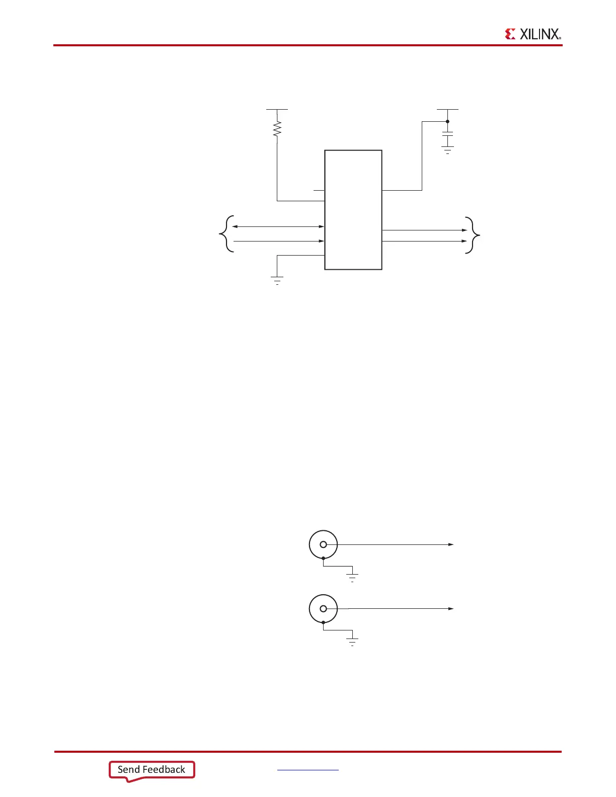
User SMA Clock Input
[Figure 1-2, callout 8]
An external high-precision clock signal can be provided to the FPGA bank 15 by
connecting differential clock signals through the onboard 50Ω SMA connectors J31 (P) and
J32 (N). The differential clock signal names are USER_SMA_CLOCK_P and
USER_SMA_CLOCK_N, which are connected to FPGA U1 pins J23 and H23 respectively.
The user-provided differential clock circuit is shown in
Figure 1-13.
Note: This user clock is input to FPGA bank 15 which is powered by VCCO_VADJ. The
VCCO_VADJ rail is typically 2.5V, but can be reprogrammed to be either 1.8V or 3.3V. The
USER_SMA_CLOCK_P/N signals should not exceed the VCCO_VADJ voltage (1.8V, 2.5V or 3.3V)
in use.
X-Ref Target - Figure 1-12
Figure 1-12: User Clock Source
UG952_c1_11_101512
GND
VCC3V3
Si570
Programmable
Oscillator
NC
OE
GND
SCL
SDA
VDD
1
2
3
8
7
6
U34
R15
4.7KΩ 5%
USER CLOCK N
C192
0.01 μF 25V
X7R
CLK-
4
5
GND
VCC3V3
CLK+
USER CLOCK P
USER CLOCK SDA
USER CLOCK SCL
10 MHz - 810 MHz
To
I
2
C
Bus Switch
(U49)
X-Ref Target - Figure 1-13
Figure 1-13: User SMA Clock Source
USER_SMA_CLOCK_P
J32
USER_SMA_CLOCK_N
GND
J31
GND
UG952_c1_12_100212
SMA
Connector
SMA
Connector