AC701 Evaluation Board www.xilinx.com 39
UG952 (v1.3) April 7, 2015
Feature Descriptions
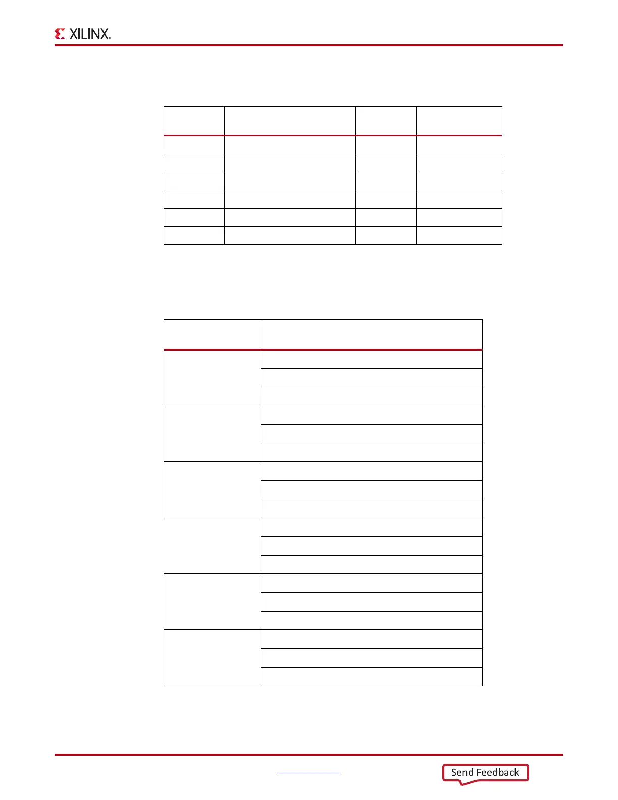
Table 1-13 lists the SFP+ module receive and transmit connections to the FPGA.
Table 1-14 lists the SFP+ module control and status connections.
Table 1-13: FPGA U1 to SFP+ Module Connections
FPGA Pin
(U1)
Schematic
Net Name
SFP+ Pin
(P5)
SFP+ Pin Name
(P5)
AD12 SFP_RX_N 12 RD_N
AC12 SFP_RX_P 13 RD_P
AD10 SFP_TX_N 19 TD_N
AC10 SFP_TX_P 18 TD_P
R18 SFP_TX_DISABLE
(1)
3 TX_DISABLE
R23 SFP_LOS
(1)
8 LOS
Notes:
1. For SFP_TX_DISABLE and SFP_LOS, the I/O standard = LVCMOS33.
Table 1-14: SFP+ Module Control and Status
SFP Control/Status
Signal
Board Connection
SFP_TX_FAULT
Test point J22
High = fault
Low = normal operation
SFP_TX_DISABLE
Jumper J6 (and FPGA pin R18)
Off = SFP disabled
On = SFP enabled
SFP_MOD_DETECT
Test point J21
High = module not present
Low = module present
SFP_RS0
Jumper J38
Jumper pins 1-2 = full receiver bandwidth
Jumper pins 2-3 = reduced receiver bandwidth
SFP_RS1
Jumper J39
Jumper pins 1-2 = full transmitter bandwidth
Jumper pins 2-3 = reduced transmitter bandwidth
SFP_LOS
Test point J20
High = loss of receiver signal
Low = normal operation