AC701 Evaluation Board www.xilinx.com 41
UG952 (v1.3) April 7, 2015
Feature Descriptions
The Ethernet connections from the XC7A200T at U1 to the 88E1116R PHY device at U12 are
listed in
Table 1-16 Ethernet PHY Connections to FPGA U1.
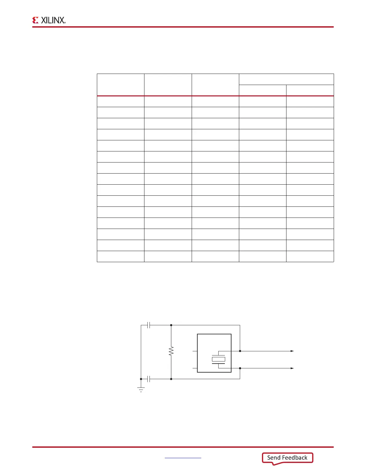
Ethernet PHY Clock Source
A 25.00 MHz, 50 ppm crystal at X1 is the clock source for the 88E1116R PHY at U12.
Figure 1-23 shows the clock source.
Table 1-16: Ethernet PHY U12 Connections to FPGA U1
FPGA Pin (U1)
Schematic Net
Name
I/O Standard
M88E1116R (U12)
Pin Pin Name
T14 PHY_MDIO LVCMOS18 45 MDIO
W18 PHY_MDC LVCMOS18 48 MDC
U22 PHY_TX_CLK LVCMOS18 60 TX_CLK
T15 PHY_TX_CTRL HSTL 63 TX_CTRL
U16 PHY_TXD0 HSTL 58 TXD0
U15 PHY_TXD1 HSTL 59 TXD1
T18 PHY_TXD2 HSTL 61 TXD2
T17 PHY_TXD3 HSTL 62 TXD3
U21 PHY_RX_CLK LVCMOS18 53 RX_CLK
U14 PHY_RX_CTRL HSTL 49 RX_CTRL
U17 PHY_RXD0 HSTL 50 RXD0
V17 PHY_RXD1 HSTL 51 RXD1
V16 PHY_RXD2 HSTL 54 RXD2
V14 PHY_RXD3 HSTL 55 RXD3
V18 PHY_RESET_B LVCMOS18 10 RESET_B
X-Ref Target - Figure 1-23
Figure 1-23: Ethernet PHY Clock Source
UG952_c1_21_100312
GND
R275
1.0M 5%
C406
18pF 50V
NPO
NC
NC
C405
18pF 50V
NPO
PHY_XTAL_OUT
GND2
GND1
X2
X1
X1
25.00 MHz
50 ppm
PHY_XTAL_IN
3
4
1
2