EasyManuals Logo
Home>Xilinx>Motherboard>AC701

Xilinx AC701 User Manual

Xilinx AC701
108 pages
To Next Page IconTo Next Page
To Previous Page IconTo Previous Page
Page #78 background imageLoading...
Page #78 background image
78 www.xilinx.com AC701 Evaluation Board
UG952 (v1.3) April 7, 2015
Chapter 1: AC701 Evaluation Board Features
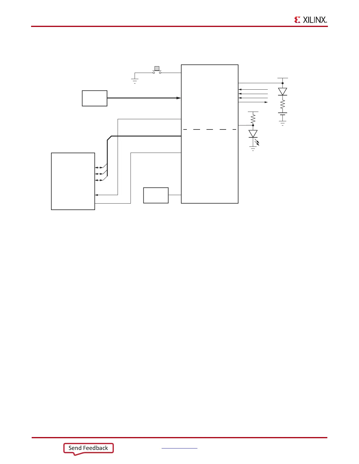
Figure 1-50 shows the Quad SPI flash memory U7 configuration circuit.
X-Ref Target - Figure 1-50
Figure 1-50: AC701 Board Quad SPI Flash Memory Configuration Circuit
UG952_c1_42_072513
DQ[1:0]
DQ2_WP
DQ3_HOLD_B
C
S-B
U7
N25Q256A13ESF40G
QUAD SPI
TCK
TMS
TDI
TDO
Bank 0
CCLK
VCCBATT
M[2:0]
DONE
PROGRAM_B
PROG_B
U1
FPGA
SW9
Bank 14
D[3:0]
FCS_B
EMCCLK
SIT8103
GND
VCC1V8
VCC3V3
R396
4.7K
GND
R396
261Ω
D6
BAS40-04
B1
DS10
GREEN
GND
U40
Oscillator
90 MHz
SW1
Mode
Switch
Send Feedback

Other manuals for Xilinx AC701

Questions and Answers:

Question and Answer IconNeed help?

Do you have a question about the Xilinx AC701 and is the answer not in the manual?

Xilinx AC701 Specifications

General IconGeneral
BrandXilinx
ModelAC701
CategoryMotherboard
LanguageEnglish

Related product manuals