AC701 Evaluation Board www.xilinx.com 9
UG952 (v1.3) April 7, 2015
Overview
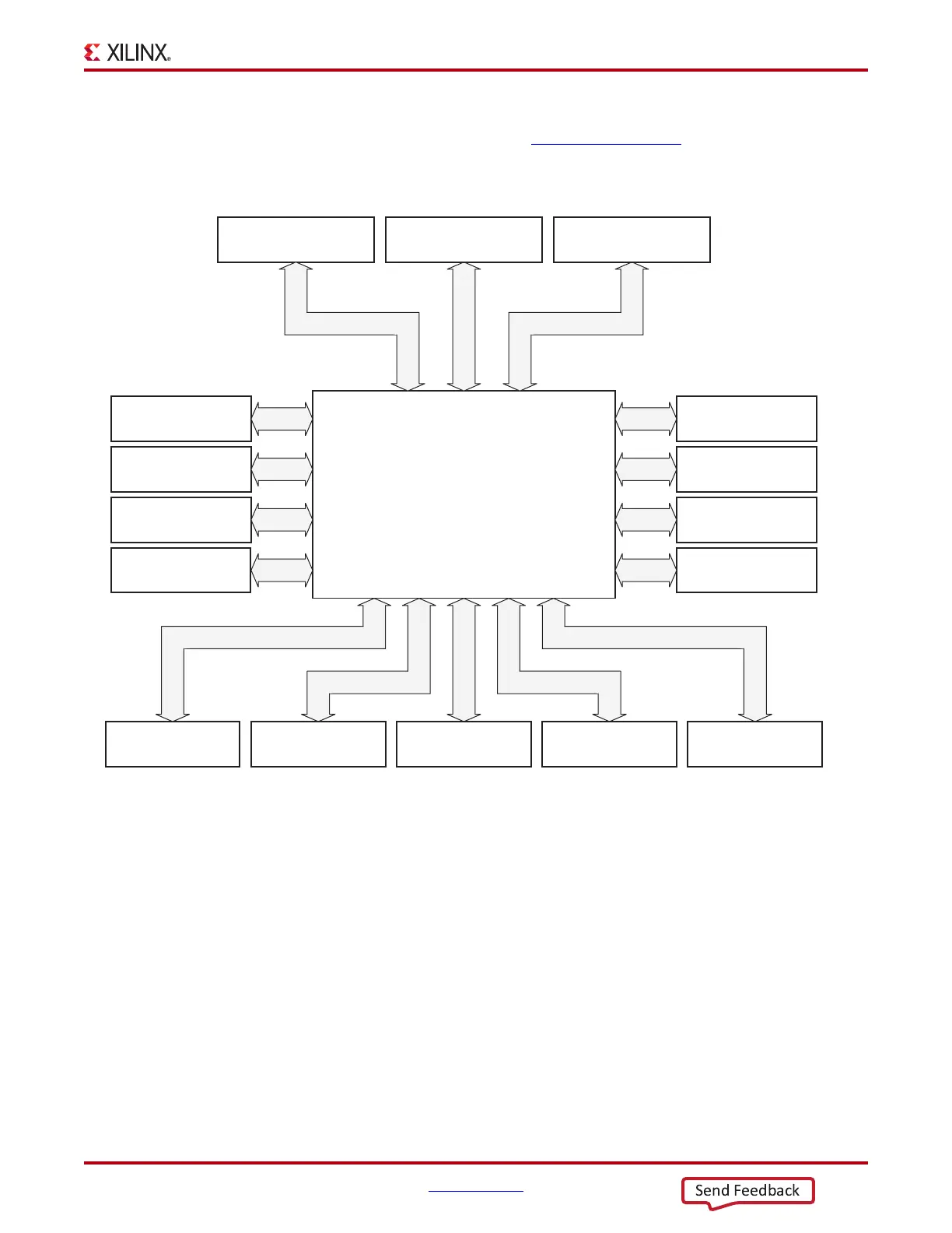
The AC701 board block diagram is shown in Figure 1-1. The AC701 board schematics
are available for download from the AC701 Evaluation Kit product page.
Caution! The AC701 board can be damaged by electrostatic discharge (ESD). Follow
standard ESD prevention measures when handling the board.
X-Ref Target - Figure 1-1
Figure 1-1: AC701 Board Block Diagram
UG952_c1_01_101512
Artix-7 FPGA
XC7A200T-2FBG676C
128 Mb Quad SPI
Flash Memory
SD Card
Interface
4-lane PCI Express
Edge Connector
LCD Display
(2 line x 16 characters)
1 KB EEPROM (I
2
C)
I
2
C Bus Switch
XADC Header
User Switches,
Buttons, and LEDs
HDMI Video
Interface
Differential Clock
GTP SMA Clock
1 GB DDR3 Memory
(SODIMM)
FMC Connector
(HPC)
10/100/1000 Ethernet
Interface
DIP Switch SW1
Config
USB-to-UART Bridge
JTAG Interface
micro-B USB Connector
SFP+ Single Cage