KCU105 Board User Guide www.xilinx.com 13
UG917 (v1.4) September 25, 2015
Chapter 1: KCU105 Evaluation Board Features
FPGA Configuration
The UltraScale FPGA is configured using either the master SPI or JTAG mode as determined
by the configuration DIP switch SW15.
Interfaces supporting these configuration modes are:
• Master SPI: Quad SPI flash memory (U35 and U36)
•JTAG:
°
Digilent USB-to-JTAG configuration module (U115)
°
Platform cable header (J3)
°
System controller (U111)
Each configuration interface corresponds to one or more configuration modes and bus
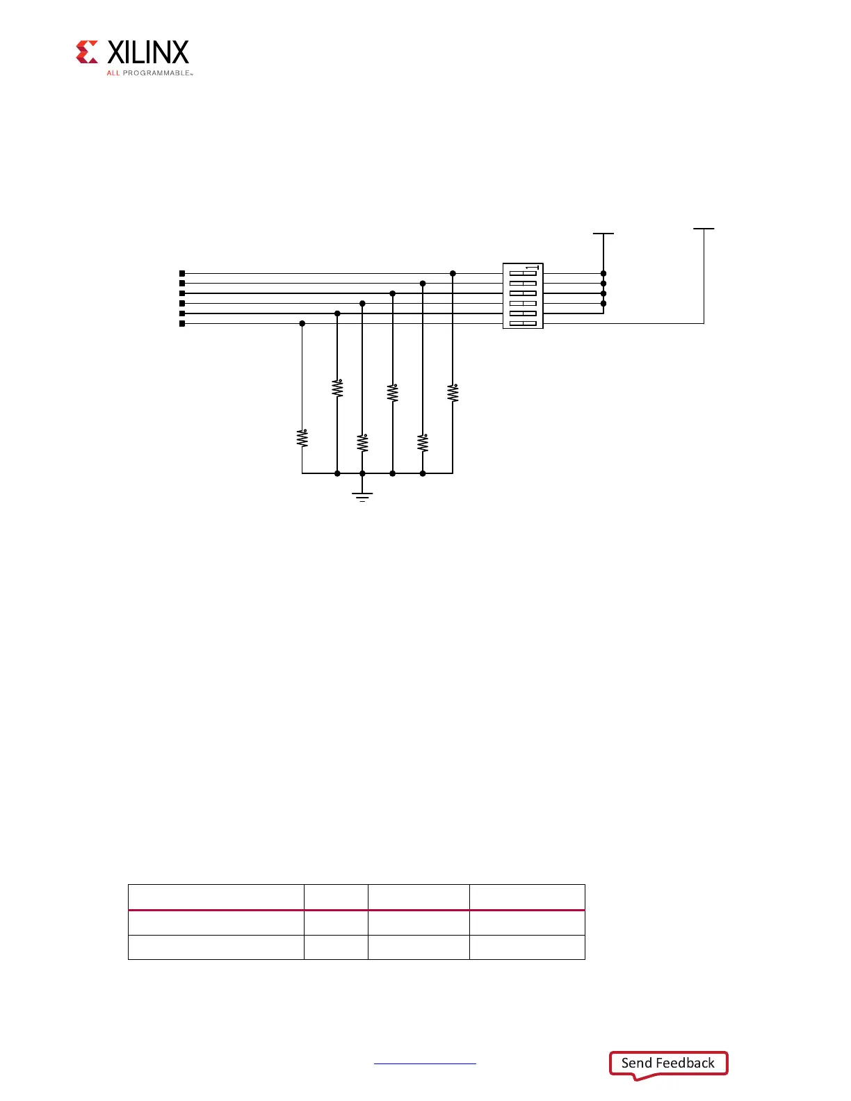
widths, as listed in Ta ble 1- 2. The FPGA mode pins M1 and M0 are hard-wired to logic 0 and
1, respectively. FPGA mode pin M2 is wired to SW15 pin 6 position 6, which has a default
setting of OPEN, enabling the M2 net to be pulled down to logic 0 (for example, the FPGA
default mode setting M[2:0] = 001, selecting Quad SPI configuration mode).
X-Ref Target - Figure 1-3
Figure 1-3: Configuration DIP Switch
Table 1-2: Configuration Modes
Configuration Mode M[2:0] Bus Width CCLK Direction
Master SPI 001 x1, x2, x4 Output
JTAG 101 x1 Not Applicable
*1'
5
5
5
5
6<6B9
6<6&7/5B02'(
6<6&7/5B02'(
6<6&7/5B02'(
6<6&7/5B02'(
5
)3*$B0
9&&9
&21),*',3
6<6&7/5B(1$%/(
6:
6'$+6%'
5
8*BB