116 MicroBlaze Development Kit Spartan-3E 1600 Edition User Guide
www.xilinx.com UG257 (v1.1) December 5, 2007
Chapter 15: Expansion Connectors
R
Three signals are reserved primarily as clock signals between the board and FX2 connector,
although all three connect to full I/O pins.
Voltage Supplies to the Connector
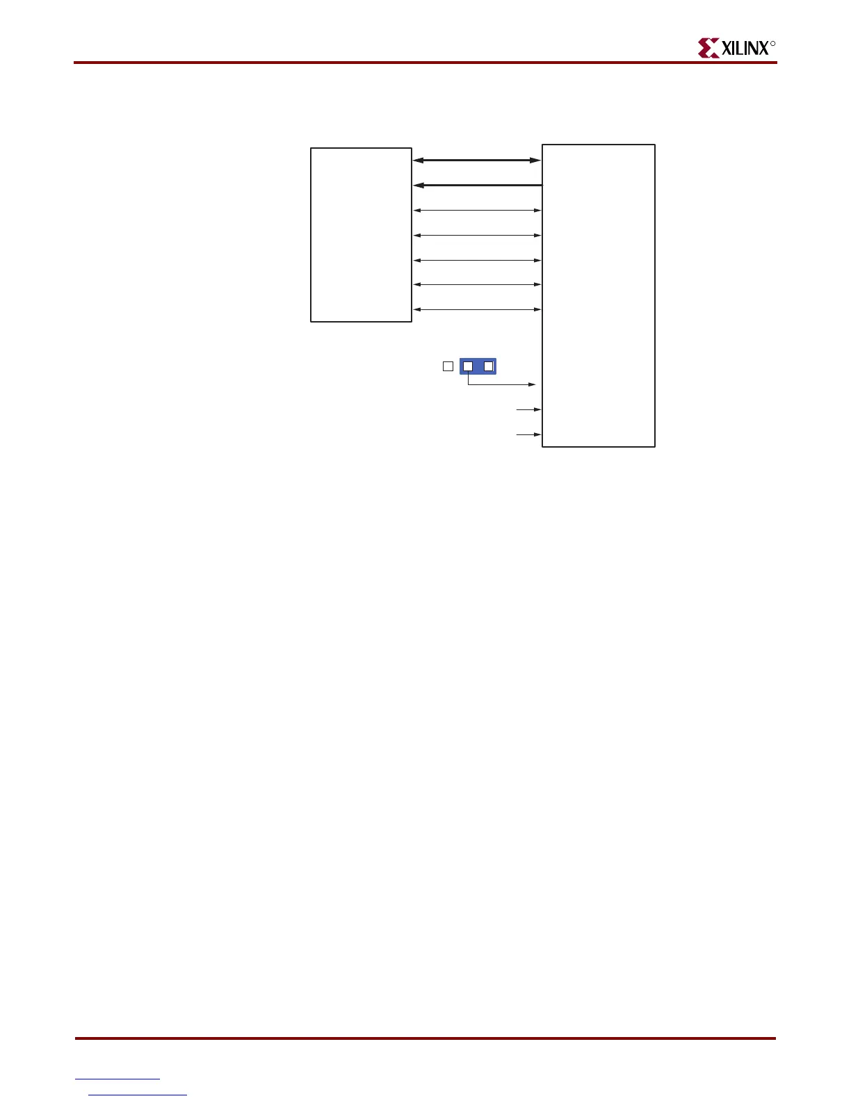
The MicroBlaze Development Kit board provides power to the Hirose 100-pin FX
connector and any attached board via two supplies (see Figure 15-2). The 5.0V supply
provides a voltage source for any 5V logic on the attached board or alternately provides
power to any voltage regulators on the attached board.
A separate supply provides the same voltage at that applied to the FPGA’s I/O Bank 0. All
FPGA I/Os that interface to the Hirose connector are in Bank 0. The I/O Bank 0 supply is
3.3V by default. However, the voltage level can be changed to 2.5V using jumper JP9. Some
FPGA I/O standards—especially the differential standards such as RSDS and LVDS—
require a 2.5V output supply voltage.
To support high-speed signals across the connector, a majority of pins on the B-side of the
FX2 connector are tied to GND.
Connector Pinout and FPGA Connections
Table 15-1 shows the pinout for the Hirose 100-pin FX2 connector and the associated FPGA
pin connections. The FX2 connect has two rows of connectors, both with 50 connections
each, shown in the table using light yellow shading.
Table 15-1 also highlights the shared connections to the eight discrete LEDs, the three 6-pin
Accessory Headers (J1, J2, and J4), and the connectorless debugging header (J6).
Figure 15-2: FPGA Connections to the Hirose 100-pin Edge Connector
Hirose 100-pin Expansion
Connector (J3)
(See Table)
FX2_IO<34:1>
Spartan-3E FPGA
FX2_IP<38:35>
(See Table)
FX2_IO<39>
5.0V
(E10)
FX2_CLKIN
(D10)
FX2_CLKOUT
(D9)
FX2_CLKIO
(See Table)
(See Table)
(B.46)
(A.47)
(B.48)
GND
3.3V2.5V
Bank 0 Supply
(JP9)
FX2_IP<40>
(C15)
(C3)
(A.45)
(A.44)
UG257_15_02_060806