MicroBlaze Development Kit Spartan-3E 1600 Edition User Guide 87
UG257 (v1.1) December 5, 2007 www.xilinx.com
Shared Connections
R
Shared Connections
Besides the connections to the FPGA, the StrataFlash memory shares some connections to
other components.
Character LCD
The LCD supports an 8-bit or a 4-bit data interface. The eight display data connections are
also shared with the SF_D<15:8> signals on the StrataFlash PROM. As shown in Table 11-2,
the FPGA controls access to the StrataFlash PROM or the character LCD using the SF_CE0
and LCD_RW signals.
Xilinx XC2C64A CPLD
The Xilinx XC2C64A CoolRunner CPLD controls the five upper StrataFlash address lines,
SF_A<24:20> during configuration. The four upper BPI-mode address lines from the
FPGA, A<23:20> are not connected. Instead, four FPGA user-I/O pins connect to the
StrataFlash PROM upper address lines SF_A<23:0>. See Chapter 16, “XC2C64A
CoolRunner-II CPLD” for more information.
The most-significant address line, SF_A<24>, is not physically used on the 16 Mbyte
StrataFlash PROM. It is provided for upward migration to a larger StrataFlash PROM in
the same package footprint. Likewsie, the SF_A<24> signal is also connected to the
FX2_IO<32> signal on the FX2 expansion connector.
SPI Data Line
The least-significant StrataFlash data line, SF_D<0>, is shared with data output signals
from serial SPI peripherals, SPI_MISO, and the serial output from the Platform Flash
PROM as shown in Table 11-3. To avoid contention, the FPGA application must ensure that
only one data source is active at any time.
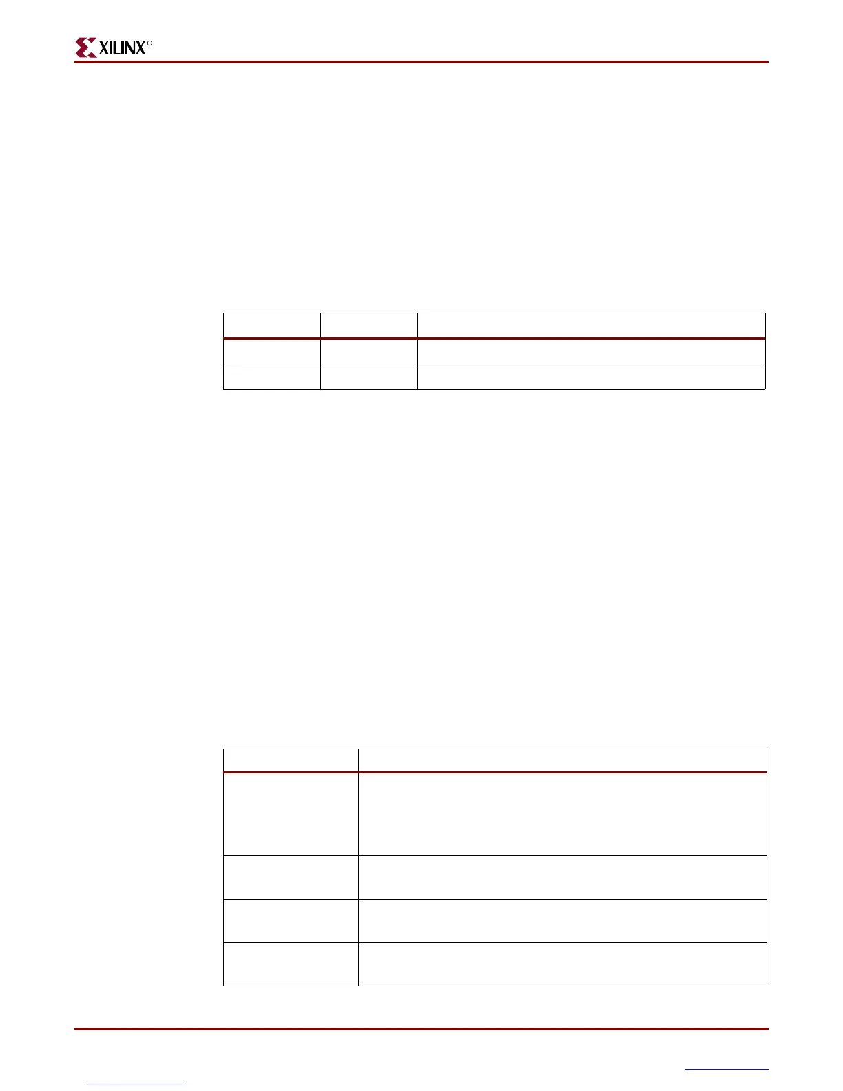
Table 1 1 -2: FPGA Control for StrataFlash and LCD
SF_CE0 LCD_RW Function
11The FPGA reads from the character LCD.
00The FPGA accesses the StrataFlash PROM.
Table 1 1 -3: Possible Contention on SPI_MISO (SF_D<0>) Data
Condition Function
FPGA_M2 = Low
FPGA_M1 = Low
FPGA_M0 = Low
INIT_B = High
Platform Flash outputs data on D0.
SF_CE0 = Low
SF_OE = Low
StrataFlash outputs data.
AD_CONV = High
SPI_SCK
Serial data is clocked out of the A/D converter
DAC_CS = Low
SPI_SCK
DAC outputs previous command in response to SPI_SCK transitions.