80 MicroBlaze Development Kit Spartan-3E 1600 Edition User Guide
www.xilinx.com UG257 (v1.1) December 5, 2007
Chapter 10: Analog Capture Circuit
R
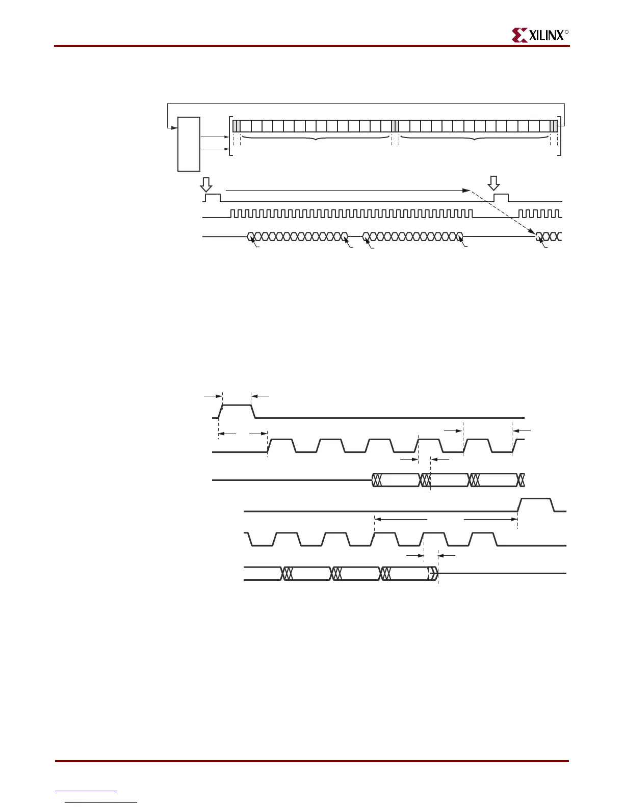
Figure 10-7 shows detailed transaction timing. The AD_CONV signal is not a traditional
SPI slave select enable. Be sure to provide enough SPI_SCK clock cycles so that the ADC
leaves the SPI_MISO signal in the high-impedance state. Otherwise, the ADC blocks
communication to the other SPI peripherals. As shown in Figure 10-6, use a 34-cycle
communications sequence. The ADC 3-states its data output for two clock cycles before
and after each 14-bit data transfer.
UCF Location Constraints
Figure 10-8 provides the User Constraint File (UCF) constraints for the amplifier interface,
including the I/O pin assignment and I/O standard used.
Figure 10-6: Analog-to-Digital Conversion Interface
Figure 10-7: Detailed SPI Timing to ADC
Spartan-3E
FPGA Master
6
0
6
1
6
2
6
3
6
4
6
5
6
6
6
7
6
8
6
9
6
10
6
11
6
12
6
13
6
0
6
1
6
2
6
3
6
4
6
5
6
6
6
7
6
8
6
9
6
10
6
11
6
12
6
13
Z
Z
Z
13
0
SPI_MISO
SPI_SCK
AD_CONV
Channel 0 Channel 0Channel 1
Sample point
Sample point
Converted data is presented with a latency of one sample.
The sampled analog value is converted to digital data 32 SPI_SCK cycles after asserting AD_CONV.
The converted values is then presented after the next AD_CONV pulse.
AD_CONV
SPI_SCK
SPI_MISO
Slave: LTC1407A-1 A/D Converter
Channel 1 Channel 0
UG257_10_06_060706
0
13
13
SPI_SCK
AD_CONV
SPI_MISO
13
12 11
High-Z
2
10
High-Z
6ns
8ns
3ns
4ns min
19.6ns min
45ns min
3
12
3
34
4
32
5
6
333130
The A/D converter sets its SDO output line to high impedance after 33 SPI_SCK clock cycles
Channel 1
Channel 0
SPI_SCK
AD_CONV
SPI_MISO
UG257_10_07_060706