MicroBlaze Development Kit Spartan-3E 1600 Edition User Guide 13
UG257 (v1.1) December 5, 2007 www.xilinx.com
R
Chapter 2
Switches, Buttons, and Knob
Slide Switches
Locations and Labels
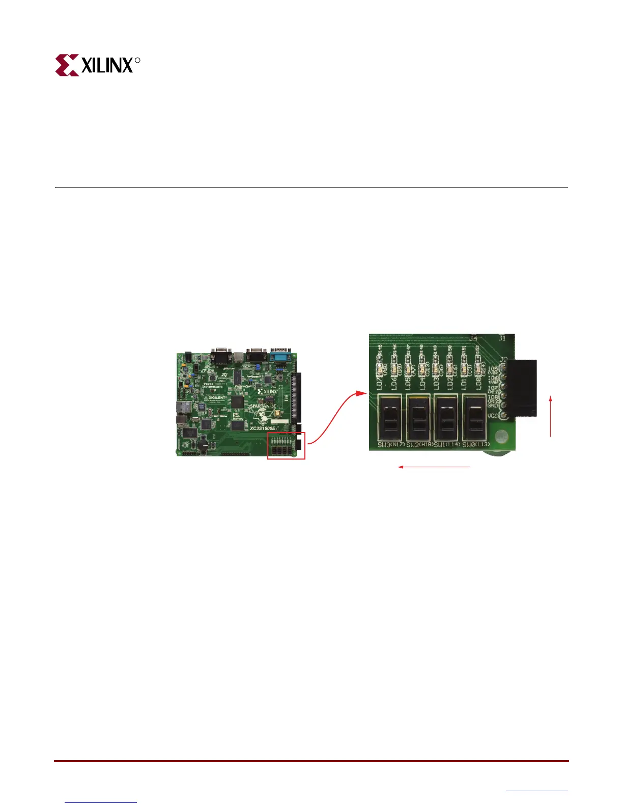
The MicroBlaze Development Kit board has four slide switches, as shown in Figure 2-1.
The slide switches are located in the lower right corner of the board and are labeled SW3
through SW0. Switch SW3 is the left-most switch, and SW0 is the right-most switch.
Operation
When in the UP or ON position, a switch connects the FPGA pin to 3.3V, a logic High.
When DOWN or in the OFF position, the switch connects the FPGA pin to ground, a logic
Low. The switches typically exhibit about 2 ms of mechanical bounce and there is no active
debouncing circuitry, although such circuitry could easily be added to the FPGA design
programmed on the board.
UCF Location Constraints
Figure 2-2 provides the UCF constraints for the four slide switches, including the I/O pin
assignment and the I/O standard used. The PULLUP resistor is not required, but it defines
the input value when the switch is in the middle of a transition.
Figure 2-1: Four Slide Switches
Spartan-3E
Development Board
HIGH
LOW
UG257_02_01_061306
SW0
SW3