MicroBlaze Development Kit Spartan-3E 1600 Edition User Guide 69
UG257 (v1.1) December 5, 2007 www.xilinx.com
R
Chapter 9
Digital to Analog Converter (DAC)
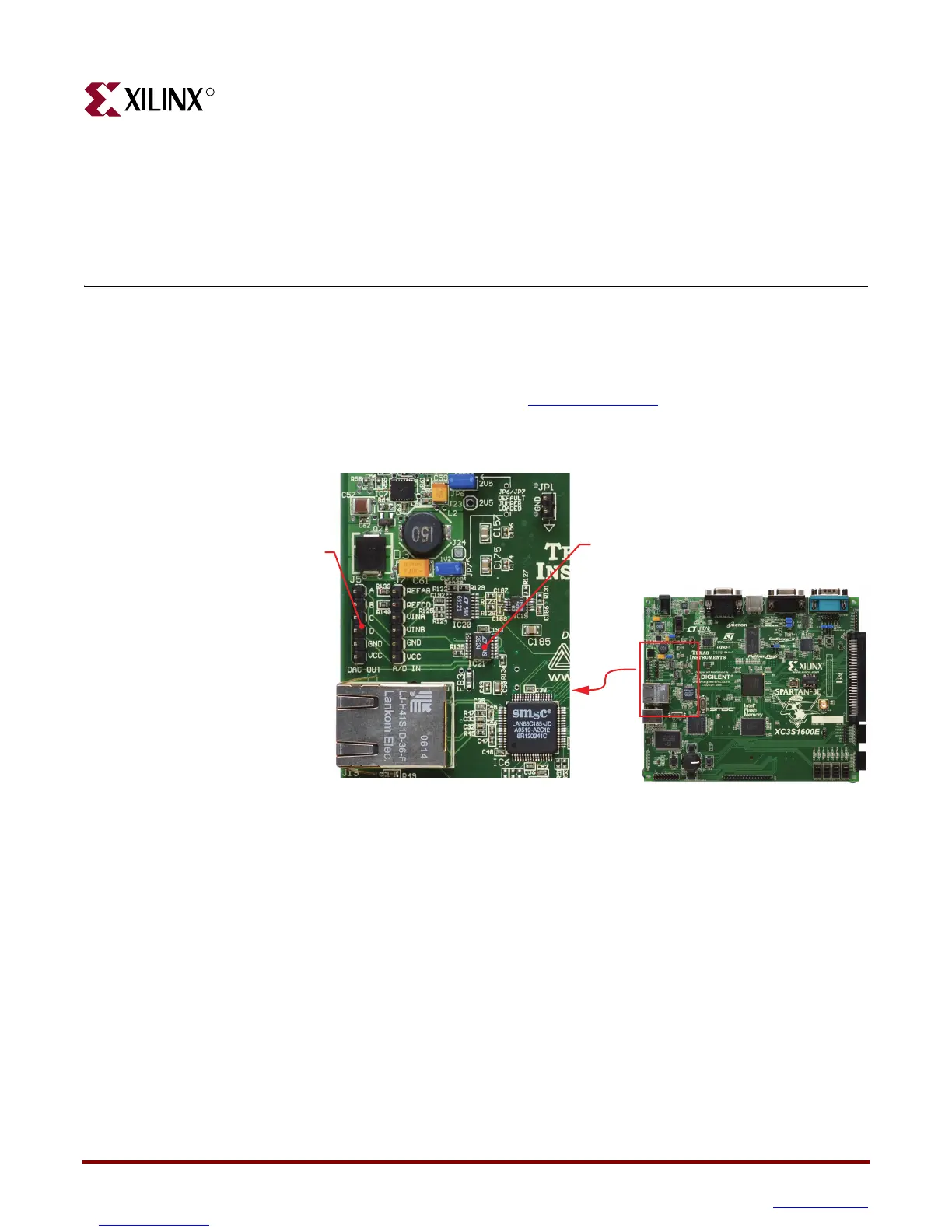
The MicroBlaze Development Kit board includes an SPI-compatible, four-channel, serial
Digital-to-Analog Converter (DAC). The DAC device is a Linear Technology LTC2624
quad DAC with 12-bit unsigned resolution. The four outputs from the DAC appear on the
J5 header, which uses the Digilent 6-pin Peripheral Module
format. The DAC and the
header are located immediately above the Ethernet RJ-45 connector, as shown in
Figure 9-1.
SPI Communication
As shown in Figure 9-2, the FPGA uses a Serial Peripheral Interface (SPI) to communicate
digital values to each of the four DAC channels. The SPI bus is a full-duplex, synchronous,
character-oriented channel employing a simple four-wire interface. A bus master—the
FPGA in this example—drives the bus clock signal (SPI_SCK) and transmits serial data
(SPI_MOSI) to the selected bus slave—the DAC in this example. At the same time, the bus
slave provides serial data (SPI_MISO) back to the bus master.
Figure 9-1: Digital-to-Analog Converter and Associated Header
Linear Tech LTC2624 Quad DAC
SPI_MOSI: (T4)
SPI_MISO: (N10)
SPI_SCK: (U16)
DAC_CS: (N8)
DAC_CLR: (P8)
Spartan-3E
Development Board
UG257_04_01_061306
6-pin DAC
Header (J5)