RocketIO™ Transceiver User Guide www.xilinx.com 109
UG024 (v3.0) February 22, 2007
PCB Design Requirements
R
An additional feature of CDR is its ability to accept an external precision clock, REFCLK,
which either acts to clock incoming data or to assist in synchronizing the derived
RXRECCLK.
For further clarity, TXUSRCLK is used to clock data from the FPGA core to the TX FIFO.
The FIFO depth accounts for the slight phase difference between these two clocks. If the
clocks are locked in frequency, then the FIFO acts much like a pass-through buffer.
PCB Design Requirements
To ensure reliable operation of the RocketIO transceivers, certain requirements must be
met by the designer. This section outlines these requirements governing power filtering
networks, high-speed differential signal traces, and reference clocks. Any designs that do
not adhere to these requirements will not be supported by Xilinx, Inc.
Power Conditioning
Each RocketIO transceiver has five power supply pins, all of which are sensitive to noise.
Table 3-5 summarizes the power supply pins, their names, and associated voltages. For
power and current requirements of each supply, refer to the data sheet (DS083
).
To operate properly, the RocketIO transceiver requires a certain level of noise isolation
from surrounding noise sources. For this reason, it is required that both dedicated voltage
regulators and passive high-frequency filtering be used to power the RocketIO circuitry.
Voltage Regulator Selection and Use
Xilinx has qualified a number of linear regulators for use with RocketIO transceivers.
RocketIO supplies must be powered by voltage regulators meeting the following criteria:
• Must be a linear or LDO regulator (switching or DC/DC converter is not acceptable).
• Must be used in the circuit given in Figure 3-7.
• Must either be a qualified linear regulator listed in Table 3-6 or meet the following
criteria:
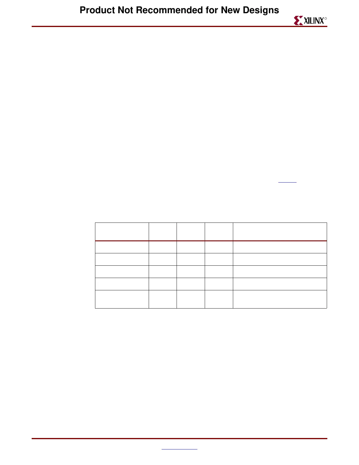
Table 3-5: Transceiver Power Supply Ranges
Supply
2.5V
±5%
1.8V -
2.625V
1.6V -
1.8V
Description
AVC CA UX RX
√
Analog RX supply
AVC CA UX TX
√
Analog TX supply
VTRX
(1)
√√
RX termination supply
VTTX
(2)
√
TX termination supply
GNDA
Analog ground for transmit and
receive analog supplies
Notes:
1.
See section “AC and DC Coupling,” page 117, and Table 3-8 for VTRX supply restrictions in AC- and
DC-coupled cases.
2. Pre-emphasis and swing settings are optimal at VTTX = 2.5V ±5%. VTTX can be powered with as low
as 1.8V in applications with data rates below 1.25 Gb/s (LVDS interfacing). Contact your Xilinx FAE
for more information on such interfaces.
Product Not Recommended for New Designs