RocketIO™ Transceiver User Guide www.xilinx.com 115
UG024 (v3.0) February 22, 2007
PCB Design Requirements
R
High-Speed Serial Trace Design
Routing Serial Traces
All RocketIO transceiver I/Os are placed on the periphery of the BGA package to facilitate
routing and inspection (since JTAG is not available on serial I/O pins). Two output/input
impedance options are available in the RocketIO transceivers: 50Ω and 75Ω. Controlled
impedance traces with a corresponding impedance should be used to connect the
RocketIO transceiver to other compatible transceivers. In chip-to-chip PCB applications,
50Ω termination and 100Ω differential transmission lines are recommended.
When routing a differential pair, the complementary traces must be matched in length to as
close a tolerance as is feasible. Length mismatches produce common mode noise and
radiation. Severe length mismatches produce jitter and unpredictable timing problems at
the receiver. Matching the differential traces to within 50 mils (1.27 mm) produces a robust
design. Since signals propagate in FR4 PCB traces at approximately 180 ps per inch, a
difference of 50 mils produces a timing skew of roughly 9 ps. Use SI CAD tools to confirm
these assumptions on specific board designs.
All signal traces must have an intact reference plane beneath them. Stripline and
microstrip geometries may be used. The reference plane should extend no less than five
trace widths to either side of the trace to ensure predictable transmission line behavior.
Routing of a differential pair is optimally done in a point-to-point fashion, ideally
remaining on the same PCB routing layer. As vias represent an impedance discontinuity,
layer-to-layer changes should be avoided wherever possible. It is acceptable to traverse the
PCB stackup to reach the transmitter and receiver package pins. If serial traces must
change layers, care must be taken to ensure an intact current return path. For this reason,
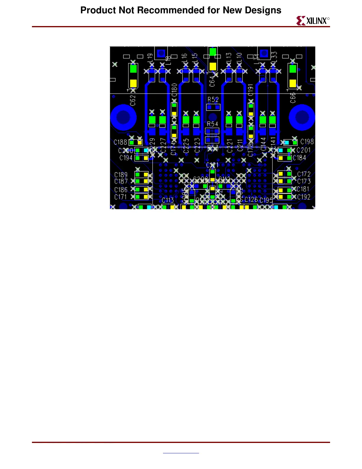
Figure 3-11: Example Power Filtering PCB Layout for Four MGTs, in Device with
External Capacitors, Bottom Layer
Product Not Recommended for New Designs