RocketIO™ Transceiver User Guide www.xilinx.com 119
UG024 (v3.0) February 22, 2007
PCB Design Requirements
R
Reference Clock
A high degree of accuracy is required from the reference clock. For this reason, it is
required that one of the oscillators listed in this section be used:
Epson EG-2121CA 2.5V (LVPECL Outputs)
See the Epson Electronics America website for detailed information. The power supply
circuit specified by the manufacturer must be used.
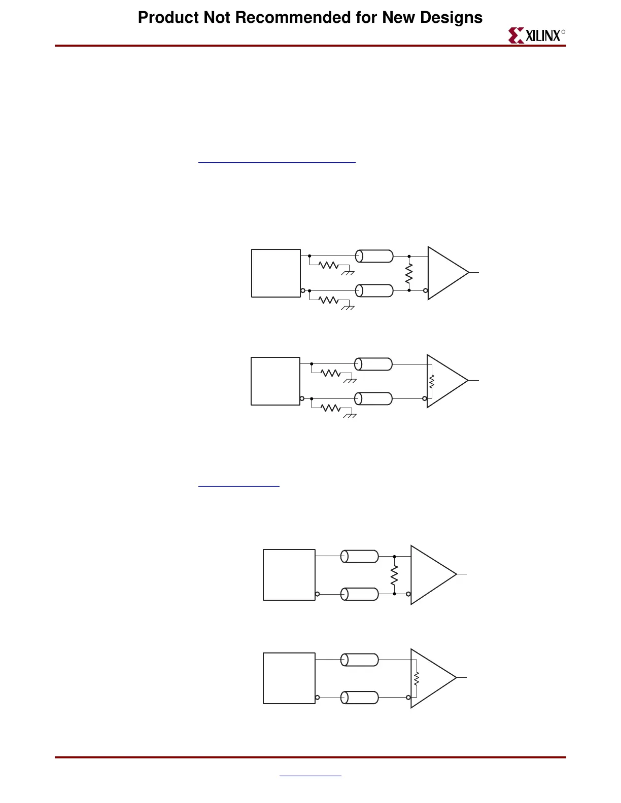
The circuit shown in Figure 3-17 must be used to interface the oscillator’s LVPECL outputs
to the LVDS or LVPECL inputs of the transceiver reference clock. Alternatively, the
LVDS_25_DT input buffers can be used to terminate the signals on-chip, as shown in
Figure 3-18.
Pletronics LV1145B (LVDS Outputs)
See the Pletronics website for detailed information.
The circuit shown in Figure 3-19 must be used to interface the oscillator’s LVDS outputs to
the LVDS inputs of the transceiver reference clock. Alternatively, the LVDS_25_DT input
buffer may be used to terminate the signals on-chip, as shown in Figure 3-20.
Figure 3-17: LVPECL Reference Clock Oscillator Interface
Figure 3-18: LVPECL Reference Clock Oscillator Interface (On-Chip Termination)
Z
0
Z
0
UG024_025a_110603
100Ω
LVDS or
LVPECL
EG2121CA
2.5V-PECL
100Ω
100Ω
Z
0
Z
0
UG024_025c_071504
EG2121CA
2.5V-PECL
100Ω
LVDS_25
_DT
100Ω
100Ω
Figure 3-19: LVDS Reference Clock Oscillator Interface
Figure 3-20: LVDS Reference Clock Oscillator Interface (On-Chip Termination)
Z
0
Z
0
UG024_025b_050102
100Ω
LVDS
LV1145B
2.5V-LVDS
Z
0
Z
0
UG024_025d_071504
100Ω
LVDS_25_DT
LV1145B
2.5V-LVDS
Product Not Recommended for New Designs