42 www.xilinx.com RocketIO™ Transceiver User Guide
UG024 (v3.0) February 22, 2007
Chapter 2: Digital Design Considerations
R
Clock Ratio
USRCLK2 clocks the data buffers. The ability to send/receive parallel data to/from the
transceiver at three different widths requires the user to change the frequency of
USRCLK2. This creates a frequency ratio between USRCLK and USRCLK2. The falling
edges of the clocks must align. Table 2-4 shows the ratios for each of the three data widths.
Digital Clock Manager (DCM) Examples
With at least three different clocking schemes possible on the transceiver, a DCM is the best
way to create these schemes.
Table 2-5 shows typical DCM connections for several transceiver clocks. REFCLK is the
input reference clock for the DCM. The other clocks are generated by the DCM. The DCM
establishes a desired phase relationship between TXUSRCLK, TXUSRCLK2, etc. in the
FPGA core and REFCLK at the pad.
NOTE: The reference clock may be any of the four MGT clocks, including the BREFCLKs.
FF672 B14/C14 C13/B13 AD14/AE14 AE13/AD13
FF896 F16/G16 G15/F15 AH16/AJ16 AJ15/AH15
FF1152 H18/J18 J17/H17 AK18/AL18 AL17/AK17
FF1148 N/A N/A N/A N/A
FF1517 E20/D20 J20/K20 AR20/AT20 AL20/AK20
FF1704 G22/F22 F21/G21 AU22/AT22 AT21/AU21
FF1696 N/A N/A N/A N/A
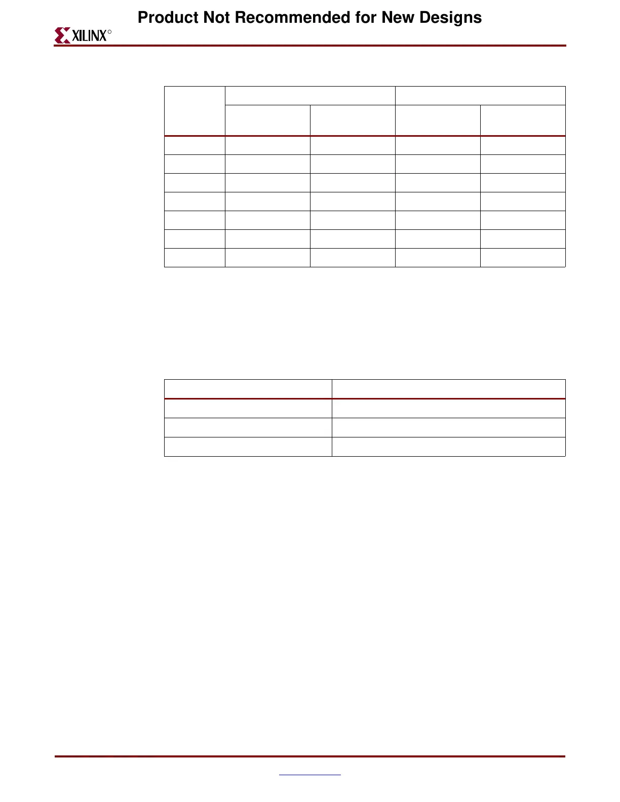
Table 2-3: BREFCLK Pin Numbers
Package
Top Bottom
BREFCLK
Pin Number
BREFCLK2
Pin Number
BREFCLK
Pin Number
BREFCLK2
Pin Number
Table 2-4: Data Width Clock Ratios
Data Width Frequency Ratio of USRCLK\USRCLK2
1 byte 1:2
(1)
2 byte 1:1
4 byte 2:1
(1)
Notes:
1. Each edge of the slower clock must align with the falling edge of the faster clock.
Product Not Recommended for New Designs