120 www.xilinx.com Virtex-5 FPGA ML561 User Guide
UG199 (v1.2.1) June 15, 2009
Appendix C: LCD Interface
R
Table C-1 summarizes the controller specifications.
The on-chip RAM size is 65 x 132 = 8580 bits.
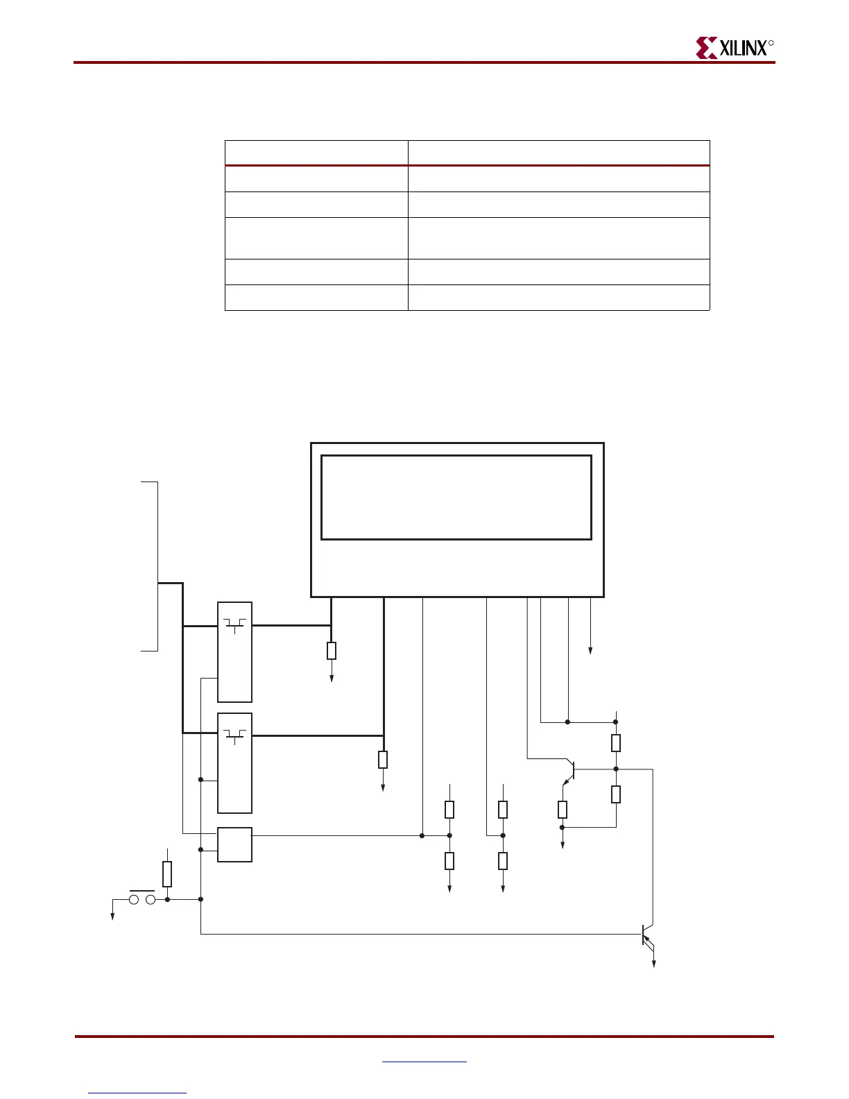
Hardware Schematic Diagram
Figure C-1 illustrates the schematic for the display.
Tab l e C -1 : Display Controller Specifications
Parameter Specification
Supply Voltage 2.4V to 3.6V (V
DD
)
LCD Driving Voltage 4V to 15V (V
LCD
=V0-V
DD
)
Power Consumption 70 μA typical (V
DD
= 3V, x4 boost, V0 = 11V,
internal supply = ON)
Sleep Mode 2 μA
Standby Mode 10 μA
Figure C-1: Display Schematic Diagram
3.3V
LCD_D[7:0]
ENA, R/W, RSEL, CS1B
LCD-BUS
DIP1_4
3.3V
Rst Gnd Vcc - +
LED
MI
3.3V
3.3V
68xx
68xx
Default = 68xx
Default =
Resistor to Gnd
Backlight ON/OFF
IC19
IC22
IC23
SamArray
UG199_C_01_050106
 Loading...


