20 www.xilinx.com Virtex-5 FPGA ML561 User Guide
UG199 (v1.2.1) June 15, 2009
Chapter 3: Hardware Description
R
DDR2 SDRAM Components
The ML561 board contains two 333 MHz Micron MT47H32M16CC-3 (16-bit) DDR2
SDRAM components that provide a 32-bit interface to FPGA #1. Each 16-bit device is
packaged in an 84-ball FBGA package, with a common address and control bus and
separate clocks and DQS/DQ signals.
QDRII SRAM
The ML561 board contains a 300 MHz QDRII SRAM interface with a 72-bit Read interface
and a 72-bit Write interface using two Samsung K7R643684M-FC30 components (x36).
They are packaged in a 165-ball FBGA package with a body size of 15 x 17 mm. These two
components share the same address/control signals but have separate clock and data
signals.
RLDRAM II Devices
The ML561 contains a 300 MHz 36-bit RLDRAM II interface using two Micron
MT49H16M18BM-25 devices (x18) packaged in a 144-ball PBGA package. They share a
common address and control bus but have separate clocks and DQS/DQ signals.
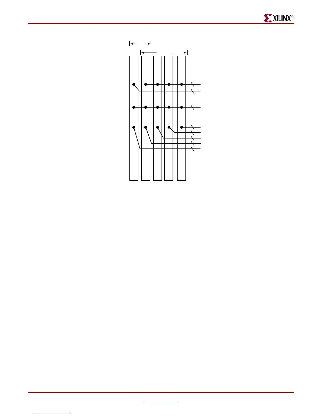
Figure 3-2: DDR2 Deep and Wide DIMM Sockets
DIMM1 (XP5)
DIMM2 (XP4)
DIMM3 (XP3)
DIMM4 (XP2)
DIMM5 (XP1)
DQ and DQS
BY0-BY7, CB0_7
DQ and DQS
BY8-BY15, CB8_15
Address and Commands
DIMM1 Control
Wide
Deep
DIMM2 Control
DIMM3 Control
DIMM4 Control
DIMM5 Control
UG199_c3_02_050106
 Loading...


