30 www.xilinx.com Virtex-5 FPGA ML561 User Guide
UG199 (v1.2.1) June 15, 2009
Chapter 3: Hardware Description
R
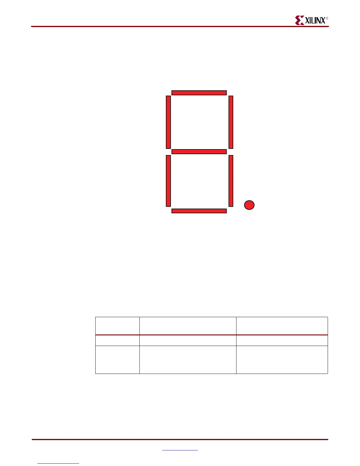
Seven-Segment Displays
One seven-segment display per FPGA (for a total of three) is available for use. The red
Stanley-Electric NAR131SB displays are active Low, using seven inputs to display a
character or number plus another input for a decimal point.
Light Emitting Diodes (LEDs)
Each FPGA is able to control four active-high green LEDs. The green is used to distinguish
the User LEDs from the blue system LEDs on the Virtex-5 FPGA ML561 Development
Board.
Pushbuttons
The ML561 board contains two momentary pushbuttons. Their functions and locations are
described in Table 3-14.
The Reset signal goes to a buffer (U32) that provides a separate copy of Reset to each
FPGA.
Figure 3-6: Seven-Segment Display Signal Mapping
7SEG_5_N 7SEG_1_N
7SEG_0_N
7SEG_6_N
7SEG_3_N
7SEG_4_N 7SEG_2_N
7SEG_DP_N
UG199_c3_06_050106
Table 3-14: User Pushbuttons
Button Description Pin Connection
SW7 PROG_B: Configure FPGA System ACE Controller: Pin 33
SW4 RESET_N: Reset the FPGA designs FPGA #1: AH14
FPGA #2: AH14
FPGA #3: AH14
 Loading...


