76 www.xilinx.com Virtex-5 FPGA ML561 User Guide
UG199 (v1.2.1) June 15, 2009
Chapter 7: ML561 Hardware-Simulation Correlation
R
DDR2 DIMM Read Operation
This subsection shows the test results for the DDR2_DIMM_DQ_BY2_B3 signal from the
DDR2 DIMM (XP2) to FPGA2 (U5) measured at 333 MHz (667 Mb/s), where the unit
interval (UI) = 1.5 ns.
To perform hardware measurements for a Read operation that is not interrupted by a Write
or a Refresh operation, the testbench on FPGA1 is controlled by the following DIP switch
(SW1) setting:
• DIP[1:2] = 2’b10 – Write once, then Read only, Refresh disabled
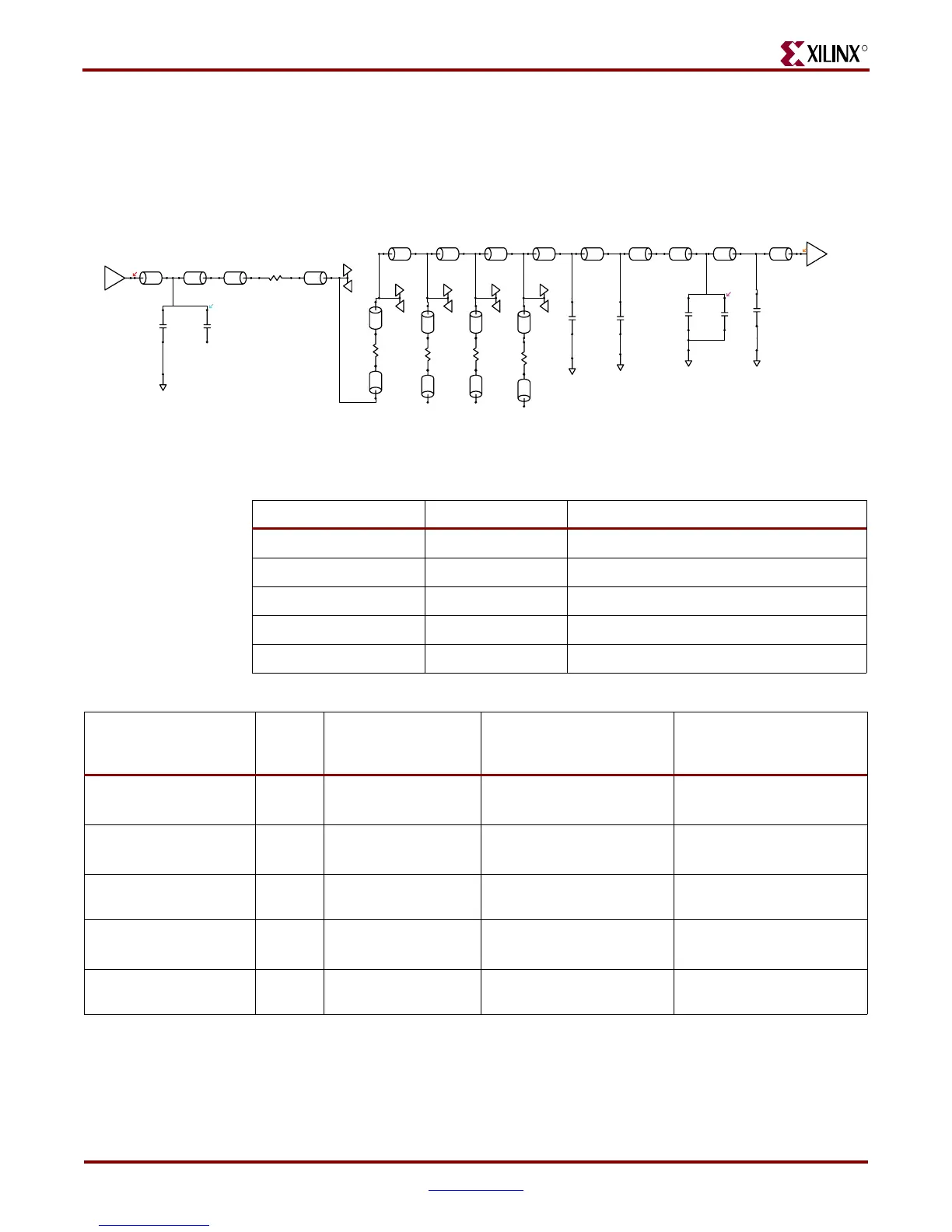
Figure 7-30: Post-Layout IBIS Schematics of the DDR2 DIMM Read Data Bit (DDR2_DIMM_DQ_B)
59.8 ohms
78.962 ps
0.490 in
MDQ19_B01
59.8 ohms
31.503 ps
0.195 in
MDQ19_B01
59.8 ohms
3.590 ps
0.022 in
MDQ19_B01
TL11TL1
U3_B01.J1
TL5 22.0 ohms
RN6_B01
MT47H64M8CB_C...
DQ6
C13
500.0 fF
17.3 fF
MDQ19_...
59.8 ohms
10.373 ps
0.064 in
DQ19_B01
TL12
J1_B01.31
????
49.8 ohms
94.605 ps
0.606 in
DDR2_DIMM_DQ_...
49.8 ohms
90.955 ps
0.582 in
DDR2_DIMM_DQ_...
49.8 ohms
90.340 ps
0.578 in
DDR2_DIMM_DQ_...
49.8 ohms
864.365 ps
5.533 in
DDR2_DIMM_DQ_...
59.1 ohms
12.486 ps
AutoPadstk_12_B...
TL15 TL16 TL17 TL18 TL19
XP5_B00.31XP4_B00.31XP3_B00.31XP2_B00.31
TL25TL23TL27TL14
????????????
????
50.3 ohms
23.650 ps
DDR2_D...
50.3 ohms
23.650 ps
DDR2_D...
50.3 ohms
23.650 ps
DDR2_D...
50.3 ohms
23.650 ps
DDR2_D...
0.0 milliohms 0.0 milliohms 0.0 milliohms 0.0 milliohms
R_00179... R7 R5 R6
DDR2_DI...
253.0 fF
50.3 ohms
23.650 ps
DQ19_B...
50.3 ohms
23.650 ps
DQ19_B...
50.3 ohms
23.650 ps
DQ19_B...
50.3 ohms
23.650 ps
DQ19_B...
TL24TL22TL26
TL13
DDR2_DI...
DDR2_DI...
DDR2_DI...
500.0 fF
C8
96.3 fF
46.4 fF
22.9 fF
U5_B00.H29
Virtex-5 FPGA
DIMM_DQ_BY2_B3
28.5 ohms
4.473 ps
0.028 in
DDR2_DIMM_DQ_...
49.1 ohms
41.316 ps
0.264 in
DDR2_DIMM_DQ_...
49.1 ohms
78.216 ps
0.501 in
DDR2_DIMM_DQ_...
71.6 ohms
22.319 ps
AutoPadstk_3_B00
TL3TL6TL7TL20
UG199_c7_30_071907
Table 7-9: Circuit Elements of DDR2 DIMM Read Data Bit
(DDR2_DIMM_DQ_BY2_B3)
Element Designation Description
Driver XP2-U3.J1 DDR2 DIMM
Receiver U5.H29 FPGA SSTL18_II_DCI_I
Probe Point C8 Via under FPGA2 (U5.H29)
PCB Termination None DCI at load
Trace Length Multiple TLs 8.975 inches
Table 7-10: DDR2 DIMM Read Operation Correlation Results
Measurement
DVW (%
UI)
ISI
(% UI)
Noise Margin
(VIH + VIL) = Total
(% of VREF)
Overshoot / Undershoot
Margin
(% of VREF)
Hardware at probe
point
904 ps
(60%)
(107 + 62) = 169 ps
(11.2%)
(242 + 258) = 500 mV
(623 + 613) = 1236 mV
(137.3%)
Simulation correlation
slow-weak corner
865 ps
(59%)
(130 + 83) = 213 ps
(14.2%)
(+292 + 298) = 590 mV
(524 + 504) = 1028 mV
(114.2%)
Correlation Delta:
HW vs. Simulation
39 ps
(2.6%)
44 ps (2.9%) 90 mV (10%) 208 mV (23.1%)
Extrapolation at IOB
slow-weak corner
1.23 ns
(82%)
(139 + 75) = 224 ps
(14.9%)
(243 + 303) = 546 mV
(60.7%)
(594 + 544) = 1138 mV
(116.5%)
Extrapolation at IOB
fast-strong corner
1.24 ns
(83%)
(131 + 60) = 191 ps
(12.7%)
(288 + 282) = 570 mV
(63.3%)
(+481 + 508) = 989 mV
(109.9%)
 Loading...


