Virtex-5 FPGA ML561 User Guide www.xilinx.com 121
UG199 (v1.2.1) June 15, 2009
Hardware Schematic Diagram
R
Peripheral Device KS0713
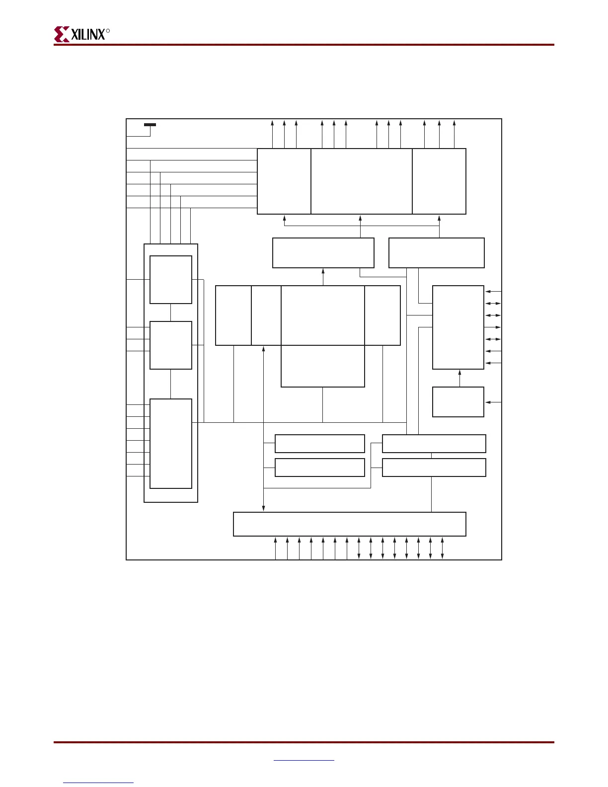
Figure C-2 is a block diagram of the Samsung KS0713.
Figure C-2: KS0713 Block Diagram
V/C
Circuit
V/R
Circuit
V/F
Circuit
Page
Address
Circuit
Line
Address
Circuit
Display Data RAM
65 x132 =
8580 Bits
132 Segment
Driver
Circuits
33 Common
Driver
Circuits
33 Common
Driver
Circuits
Column Address
Circuit
Segment Controller Common Controller
I/O
Buffer
KS0713 Samsung
VDD
VSS
CS1B
RS
E_RD
RW_WR
PS
RESETB
MI
DB7 (SID)
MPU Interface (Parallel & Serial)
Bus Holder
Oscillator
Display
Timing
Generator
Circuit
Status Register
Instruction Decoder
Instruction Register
DB6 (SCLK)
DB5
DB4
DB3
DB2
DB1
DB0
UG199_C_02_050106
 Loading...


