12 www.xilinx.com Virtex-5 FPGA ML561 User Guide
UG199 (v1.2.1) June 15, 2009
Chapter 1: Introduction
R
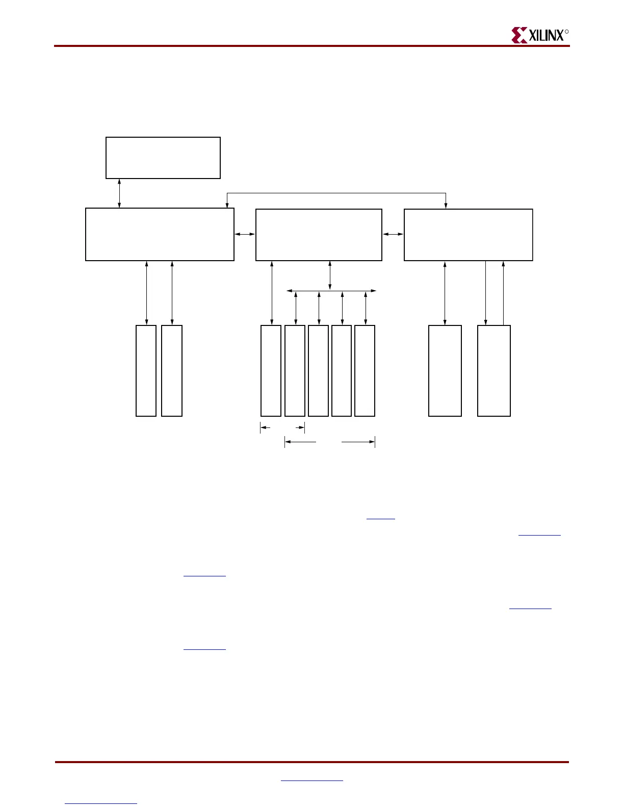
Virtex-5 FPGA ML561 Memory Interfaces Development Board
A high-level functional block diagram of the Virtex-5 FPGA ML561 Memory Interfaces
Development Board is shown in Figure 1-1.
The Virtex-5 FPGA ML561 Development Board includes the following major functional
blocks:
• Three XC5VLX50T-FFG1136 FPGAs (see D
S100, Virtex-5 Family Overview)
• DDR400 components: 128 MB (32M x 32 bits) at 200 MHz clock speed. See XAPP851,
DDR SDRAM Controller Using Virtex-5 FPGA Devices.
• DDR2 DIMM: Five PC2-5300 DIMM sockets for up to 2 GB (128M x 144 bits). See
XAPP85
8, High-Performance DDR2 SDRAM Interface in Virtex-5 Devices.
• DDR2-667 components: 64 MB (16M x 32 bits) at 333 MHz clock speed
• QDRII memory: 16 MB (2M x 72 bits) at up to 300 MHz clock speed. See XAPP853
,
QDR II SRAM Interface for Virtex-5 Devices.
• RLDRAM II memory: 64 MB (16M x 36 bits) at up to 300 MHz clock speed. See
XAPP852
, RLDRAM II Memory Interface for Virtex-5 FPGAs.
• One DB9-M RS-232 port and one USB 2.0 port
• A System ACE™ CompactFlash (CF) Configuration Controller that allows storing
and downloading of up to eight FPGA configuration image files
• On-board power regulators with ±5% output margin test capabilities
Figure 1-1: Virtex-5 FPGA ML561 Development Board Block Diagram
DDR2 DIMM
72
72
RLDRAM II
(CIO)
36
QDRII SRAM
DDR2 SDRAM
32
32
FPGA #1
XC5VLX50T/
FFG1136
FPGA #2
XC5VLX50T/
FFG1136
DDR400 SDRAM
SSTL18/SSTL2 SSTL18 HSTL
External Interfaces:
System ACE Controller,
USB, RS-232, LCD
DDR2 DIMM
DDR2 DIMM
DDR2 DIMM
DDR2 DIMM
72
72
UG191_c1_01_020807
FPGA #3
XC5VLX50T/
FFG1136
WIDE
DEEP
 Loading...


