EasyManuals Logo

Xilinx Virtex-5 FPGA ML561 User Manual

Xilinx Virtex-5 FPGA ML561
140 pages
To Next Page IconTo Next Page
To Previous Page IconTo Previous Page
Page #13 background imageLoading...
Page #13 background image
Virtex-5 FPGA ML561 User Guide www.xilinx.com 13
UG199 (v1.2.1) June 15, 2009
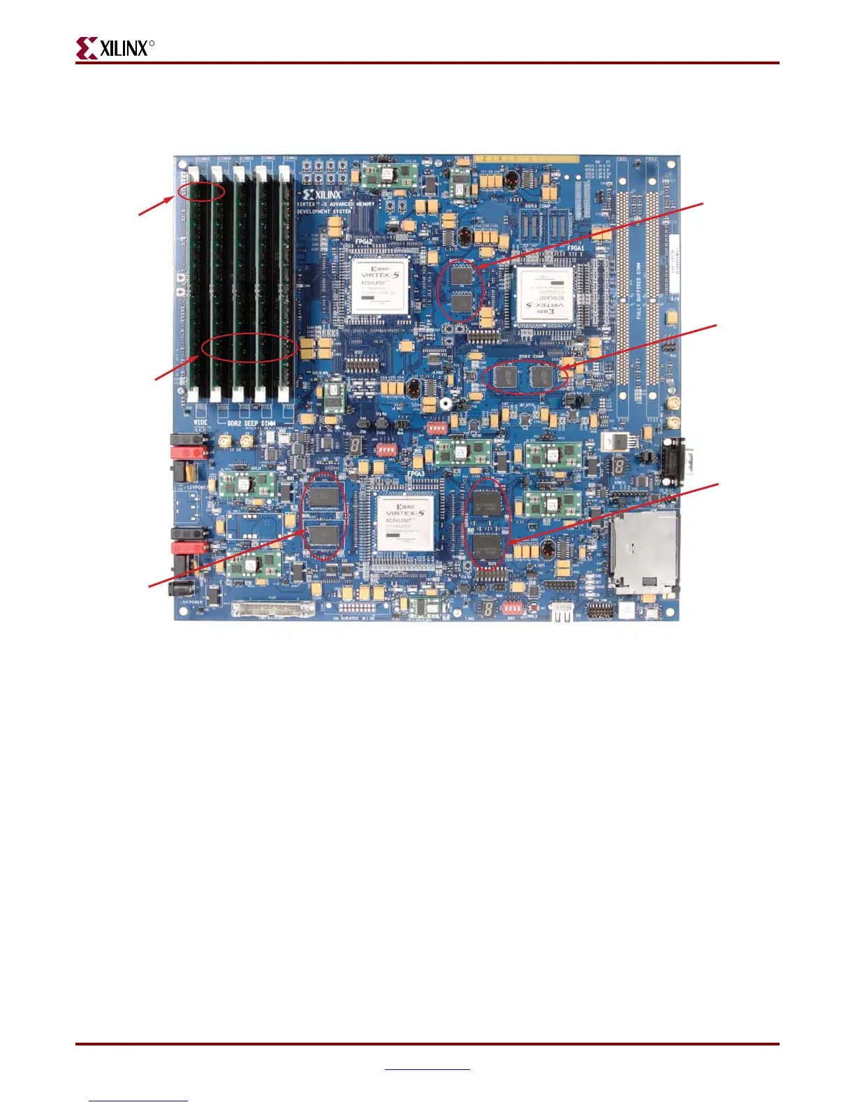
Virtex-5 FPGA ML561 Memory Interfaces Development Board
R
Figure 1-2 shows the Virtex-5 FPGA ML561 Development Board and indicates the
locations of the resident memory devices.
Figure 1-2: Virtex-5 FPGA ML561 Development Board
S A i l N 10 t hit / d h d F/L
DDR2
SDRAM
DIMM
32-bit
DDR400
SDRAM
32-bit
DDR2
SDRAM
72-bit
QDRII
SRAM
36-bit
RLDRAM II
144 bits wide
72 bits wide,
up to 4 deep
UG199_c1_02_050106

Table of Contents

Questions and Answers:

Question and Answer IconNeed help?

Do you have a question about the Xilinx Virtex-5 FPGA ML561 and is the answer not in the manual?

Xilinx Virtex-5 FPGA ML561 Specifications

General IconGeneral
BrandXilinx
ModelVirtex-5 FPGA ML561
CategoryMotherboard
LanguageEnglish

Related product manuals