Virtex-5 FPGA ML561 User Guide www.xilinx.com 123
UG199 (v1.2.1) June 15, 2009
Hardware Schematic Diagram
R
Controller – Operation
The pixels for the LCD panel are stored in the controller data RAM. This RAM is a 65-row
by 132-column array. Each display pixel is represented by a single bit in the RAM array.
The interface to the RAM array goes through the 8-bit (DB0 – DB7) LCD interface.
Therefore, the 65-bit rows are split into eight pages of eight lines. The ninth page is a single
line page (DB0 only).
Interface designs can read from or write to the RAM array.
The display page is changed through the 4-bit page address register.
The column address (line address) is set with a two-byte register access. The line address
corresponds to the first line that is going to be displayed on the LCD panel. This address is
located in a 6-bit address register.
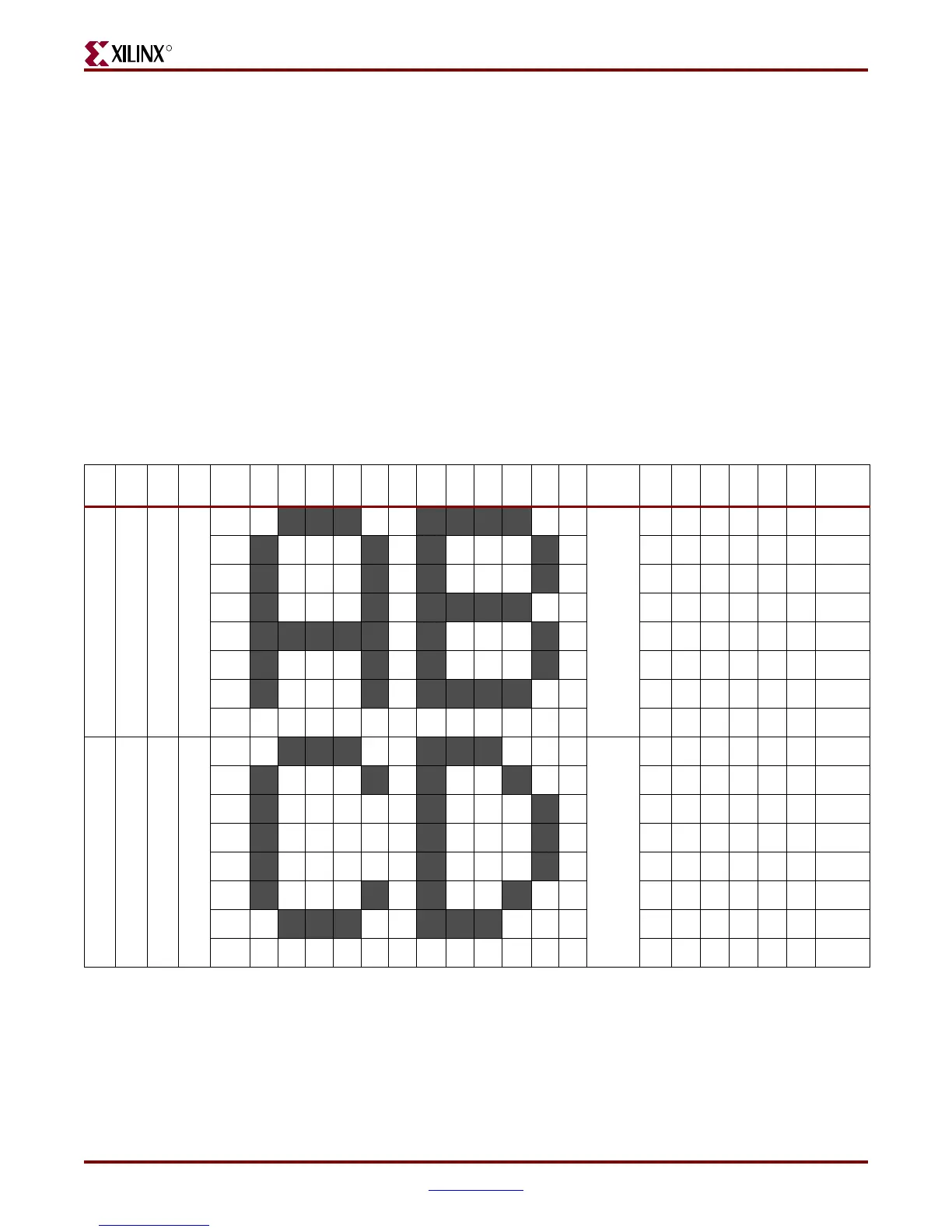
The RAM array is configured such that there are two characters per row (page), where each
character pair uses eight rows of the display panel. Table C-2 shows the input data bytes,
address lines, ADC control, and LCD outputs (segments).
Table C-2: LCD Panel
DB3 DB2 DB1 DB0 Data
Line
Address
0000
DB0
Page 0
00H
DB1
01H
DB2
02H
DB3
03H
DB4
04H
DB5
05H
DB6
06H
DB7
07H
0001
DB0
Page 1
08H
DB1
09H
DB2
0AH
DB3
0BH
DB4
0CH
DB5
0DH
DB6
0EH
DB7
0FH
 Loading...


