EasyManuals Logo

Xilinx Virtex-5 FPGA ML561 User Manual

Xilinx Virtex-5 FPGA ML561
140 pages
To Next Page IconTo Next Page
To Previous Page IconTo Previous Page
Page #139 background image
Virtex-5 FPGA ML561 User Guide www.xilinx.com 139
UG199 (v1.2.1) June 15, 2009
Hardware Schematic Diagram
R
Array Connector Numbering
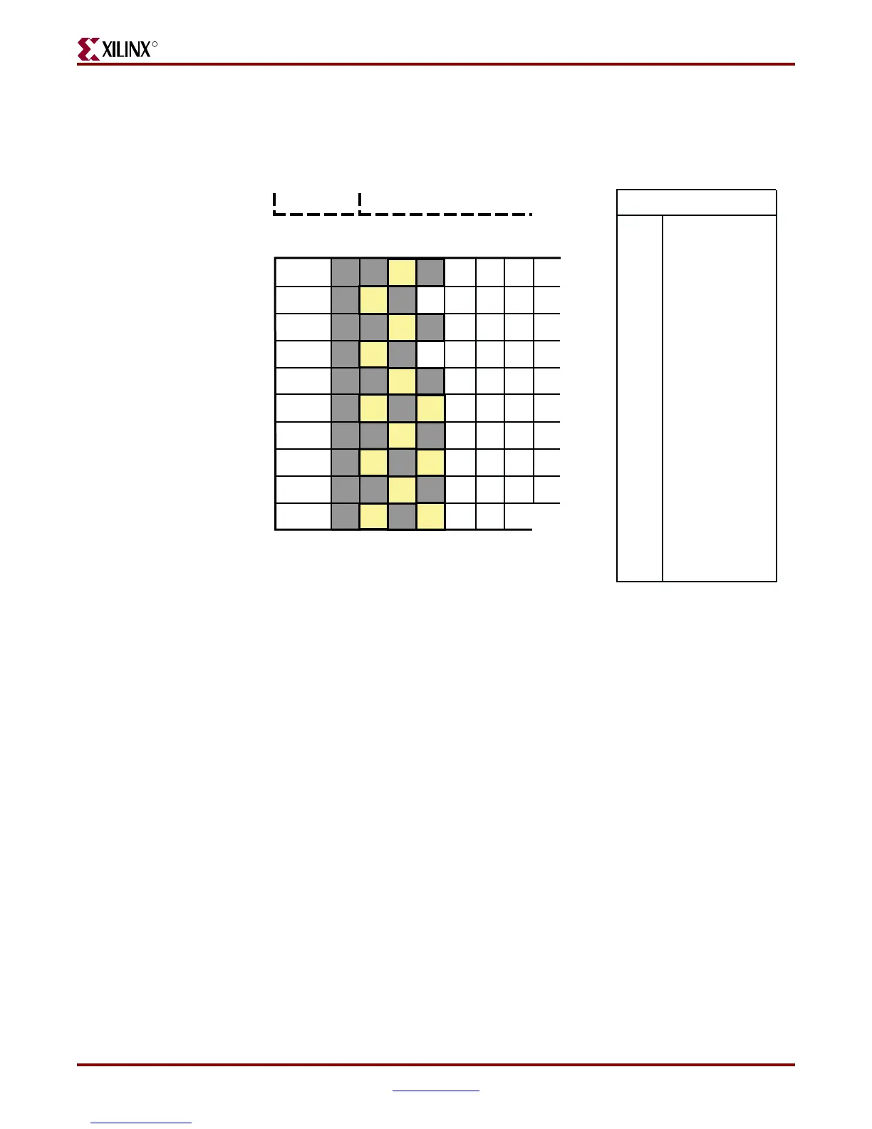
Figure C-12 shows the LCD connections for Bank 0.
Figure C-12: LCD Connections (Bank 0)
Bank 0
Connector Pin
ABCDE FGH I
D9 LCD_D0
10
D7 LCD_D4
9
D5 LCD_D5
8
D3 LCD_D6
7
D1 LCD_D7
6
E10 LCD_RST
5
E8 LCD_D1
4
E6 LCD_D2
3
E4 LCD_D3
2
E2 LCD_ENA
1
F5 LCD_R/W
F3 LCD_RSEL
Connector J32
F1 LCD_CS1B
UG199_C_12_050106

Table of Contents

Questions and Answers:

Question and Answer IconNeed help?

Do you have a question about the Xilinx Virtex-5 FPGA ML561 and is the answer not in the manual?

Xilinx Virtex-5 FPGA ML561 Specifications

General IconGeneral
BrandXilinx
ModelVirtex-5 FPGA ML561
CategoryMotherboard
LanguageEnglish

Related product manuals