Virtex-5 FPGA ML561 User Guide www.xilinx.com 27
UG199 (v1.2.1) June 15, 2009
External Interfaces
R
External Interfaces
The external interfaces of the Virtex-5 FPGA ML561 Development Board are described in
this section.
RS-232
The ML561 board provides an RS-232 serial interface using a Maxim MAX3316ECUP
device. The maximum speed of this device is 460 Kbps.
Hooks are provided to connect and disconnect FPGAs to the RS-232 serial interface, by
placing jumpers on headers based on the FPGA involved in the communication. Only one
FPGA is allowed in the communication, and others must be disconnected before operation.
The ML561 toolkit CD contains code to implement a UART core in one FPGA for
interfacing with a host PC.
The RS-232 interface is accessible through a male DB-9 serial connector (P73).
USB
Full-speed (12 Mbps) USB functionality is proved using a Silicon Laboratories CP2102-GM
USB to RS-232 Bridge. RS-232 and USB signals are converted between one another so a
RS-232 core needs to be implemented in the FPGA for communication. A level translator is
used to convert between the 2.5V I/O of the FPGA and the 3.3V I/O the CP2102 uses.
Hooks are provided to connect and disconnect FPGAs to the USB connection, by placing
jumpers on headers based on the FPGA involved in the communication. Only one FPGA is
allowed in the communication, and others must be disconnected before operation.
The USB interface is accessible through a female ‘A’ USB connector (J29).
Clocks
The ML561 board contains a 200 MHz LVPECL clock oscillator and connectors for external
clock inputs for use as system clocks (J19 and J20). The GTP transceivers use their own
clock source that can be provided through SMA connectors on the board (J16 and J21).
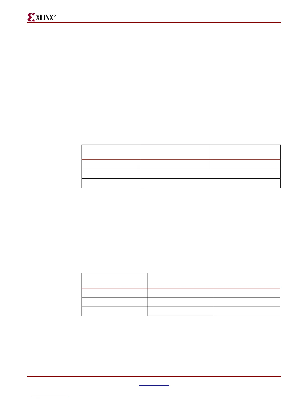
Table 3-8: RS-232 Jumper Settings
To Connect FPGA # to
DB-9 (P73)
TX RX
FPGA #1 P52 Pin 2 -> P52 Pin 1 P53 Pin 2 -> P53 Pin 1
FPGA #2 P52 Pin 2 -> P51 Pin 1 P53 Pin 2 -> P54 Pin 1
FPGA #3 P52 Pin 2 -> P52 Pin 3 P53 Pin 2 -> P53 Pin 3
Table 3-9: USB Jumper Settings
To Connect FPGA # to DB-9
(J29)
TX RX
FPGA #1 P36 Pin 2 -> P36 Pin 1 P22 Pin2 -> P22 Pin 1
FPGA #2 P36 Pin 2 -> P35 Pin 1 P22 Pin2 -> P23 Pin 1
FPGA #3 P36 Pin 2 -> P36 Pin 3 P22 Pin2 -> P22 Pin 3
 Loading...


